Semiconductor giant Intel has revealed its roadmap for process technologies, which will see 10nm, 7nm and 5nm released beginning in 2015.
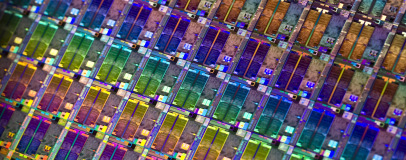
In semiconductor manufacturing, process is king: the term refers to how chip designs are shrunk from their giant human-viewable schematics down to teeny-tiny production parts with components several times thinner than a human hair. The better a company's process, the smaller the final chip; the smaller the final chip, the better the performance. Smaller process nodes also mean more chips from a particular silicon wafer, albeit tempered with the usual yield problems as issues with new process nodes are ironed out.
The majority of the industry is working on a 22nm process at present, including Intel's recently-launched Ivy Bridge processors. The next step for the semiconductor industry is 14nm, which Intel is planning to introduce with its Broadwell processors - the successor to the new microarchitecture Haswell parts, based on the same 22nm process as Ivy Bridge as part of Intel's 'tick-tock' development cycle.
All companies in the semiconductor industry are looking beyond 14nm, however - and Intel is no exception. According to slides obtained by X-bit Labs, Intel has already begun research on sub-14nm processors with a view to getting 10nm parts into development for a 2015 roll-out.
According to the research and development pipeline espoused by the company's slides, 2015 will see the production of semiconductor components based on a 10nm process size, quickly followed by 7nm and 5nm parts.
The company has an uphill struggle ahead of it, however: the smaller the process, the larger the challenge. As the component sizes decrease and the gaps between components get smaller, numerous issues raise their heads. The biggest of these, current leakage, calls for a radical rethink to how semiconductors are designed in order to smash what has been termed the '10nm physical gate length barrier.'
Some companies have already developed prototype technology for the sub-10nm process, including IBM's carbon nanotube transitor, which is running in the lab based on a 9nm process size. Intel, however, isn't detailing the precise route its own research is taking, except to explain that it's in the process of researching new lithography, materials and interconnect techniques to address the issues of shrinking component sizes.
Intel's slide deck also explains that its 14nm production, due to begin in 2013 for the Broadwell family, will take place in its D1X Oregon, Fab 42 Arizona and Fab 24 Ireland facilities following 22nm upgrades to the D1D/C Oregon, Fab 32/12 Arizona and Fab 28 Israel plants.
Should Intel hit its schedule of a 10nm part by 2015, it will likely find itself ahead of its rivals in process technology - a move which will do nothing to lessen the company's growing dominance of the mainstream processor industry.


MSI MPG Velox 100R Chassis Review
October 14 2021 | 15:04

Want to comment? Please log in.