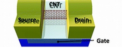
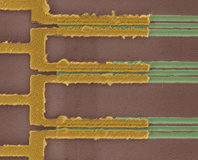
Researchers at IBM have produced what they claim is the first experimental evidence of a transistor material that will be viable at process sizes of below 10 nanometres: carbon nanotubes.
As process sizes shrink and components become packed ever more densely, several challenges present themselves. Not least of these is current leakage, which confuses nearby transistors and corrupts the signal, as Intel researchers found in a white paper (PDF) detailing the struggles with smashing what they called the '10nm physical gate length barrier.'
Shrinking process size is vital in continuing the trend for increasing semiconductor complexity: only by reducing the size of transistors and the spaces between them can increasing numbers be fitted efficiently into equivalent die sizes. The process is so important, in fact, that it forms a central part of Intel's 'tick-tock' development cycle: one year a 'tick' introduces a refinement into the processor's architecture, while the following year a 'tock' boosts performance with a move to a smaller process size.
According to a paper published in the Nano Letters journal, IBM believes it has found a way to effectively bypass the 10nm barrier: by replacing silicon with carbon nanotubes.
It's not the first suggestion for the move to sub-10nm process sizes. Intel's whitepaper, written when 130nm was the norm, looked to the tri-gate transistor technology the company is only now implementing in Ivy Bridge as a possible solution to the problem. Where Ivy Bridge is a 22nm technology and tri-gate as yet unproven at significantly smaller process sizes, however, IBM's carbon nanotube technology is already working at 9nm.
'Although carbon nanotube (CNT) transistors have been promoted for years as a replacement for silicon technology, there is limited theoretical work and no experimental reports on how nanotubes will perform at sub-10nm channel lengths,' the team explains in the paper's abstract. 'In this manuscript we demonstrate the first sub-10 nm CNT transistor, which is shown to outperform the best competing silicon devices with more than four times the diameter-normalized current density (2.41 mA/μm) at a low operating voltage of 0.5 V. The superior low-voltage performance of the sub-10 nm CNT transistor proves the viability of nanotubes for consideration in future aggressively scaled transistor technologies.'
While IBM's work on carbon nanotube field effect transistors (CNFET) is impressive, it's far from ready for commercialisation. With Intel already going to market with its tri-gate take on the FinFET concept, there's plenty of time for solutions to silicon's leakage issues to be found in order to avoid a change of material when it comes time to release sub-10nm parts into the market.
Do you think future chips will be based on carbon, silicon, or something else entirely? Share your thoughts over in the forums.


MSI MPG Velox 100R Chassis Review
October 14 2021 | 15:04

Want to comment? Please log in.