Manufacturer claims sub-20nm via breakthrough
July 11, 2012 | 10:44
Companies: #applied-materials #via
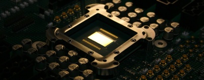
Applied Materials, equipment maker for the semiconductor, flat panel display and photovoltaic markets, has announced a new manufacturing technique which it claims will enable chipmakers to build interconnects far smaller than the current 20nm limit.
Announced at the Semicon West event late yesterday, Applied Materials' Endura Amber system promises to shrink copper interconnects in semiconductors to 10nm or less - a critical step in keeping Moore's Law alive and dropping feature sizes on future processors.
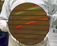
Although it's not obvious to look at them, a modern semiconductor can contain more than 60 linear miles of copper wiring across as many as 10 billion vertical connections. As process sizes shrink and increasing features are added to chips, that figure is only going to rise - and that's a real problem.
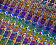
Where the interconnects meet the chip features, the wiring needs to be the same size. The result: tiny copper wires just 20nm wide for the latest generation of NAND flash parts. Creating these interconnects at such a small size causes real problems, largely due to bubbles forming as the small holes are filled with copper to create the connection. Back when interconnects were larger, these small bubbles didn't cause too much of a problem - but below 20nm a single bubble in a single interconnect can render a chip useless, meaning yields drop through the floor.
'The Applied Endura Amber system delivers a breakthrough solution for scaling interconnects beyond the 20nm node while maintaining good production yields,' claimed Sundar Ramamurthy, vice president and general manager of Applied Materials' metal deposition business unit, at the Semicon West announcement. 'Applied has extended its leading PVD technology with a unique system that achieves rapid, void-free fill of these structures at virtually any device node. We're seeing strong customer momentum for the Amber system with more than 30 chambers already in the field. Systems are already qualified as tool of record at leading logic and memory device manufacturers,' he added, without naming names.
The Amber Endura system works by filling the interconnect holes - known as vias - in as normal using a physical vapour deposition (PVD) technique, but then heating the chip to allow the capillary action of the tiny holes to draw the now-liquid copper up from the bottom. The result, Applied Materials claims, is a void-free fill with no cavitation issues. Thus far, Applied is the only company to be attempting a joint PVD-and-heating system for the creation of interconnects.
Although the company claims to be working with some of the world's leading semiconductor companies, it has yet to announce any customers that have used the Amber Endura system to fabricate a shipping product.
Announced at the Semicon West event late yesterday, Applied Materials' Endura Amber system promises to shrink copper interconnects in semiconductors to 10nm or less - a critical step in keeping Moore's Law alive and dropping feature sizes on future processors.
Although it's not obvious to look at them, a modern semiconductor can contain more than 60 linear miles of copper wiring across as many as 10 billion vertical connections. As process sizes shrink and increasing features are added to chips, that figure is only going to rise - and that's a real problem.
Where the interconnects meet the chip features, the wiring needs to be the same size. The result: tiny copper wires just 20nm wide for the latest generation of NAND flash parts. Creating these interconnects at such a small size causes real problems, largely due to bubbles forming as the small holes are filled with copper to create the connection. Back when interconnects were larger, these small bubbles didn't cause too much of a problem - but below 20nm a single bubble in a single interconnect can render a chip useless, meaning yields drop through the floor.
'The Applied Endura Amber system delivers a breakthrough solution for scaling interconnects beyond the 20nm node while maintaining good production yields,' claimed Sundar Ramamurthy, vice president and general manager of Applied Materials' metal deposition business unit, at the Semicon West announcement. 'Applied has extended its leading PVD technology with a unique system that achieves rapid, void-free fill of these structures at virtually any device node. We're seeing strong customer momentum for the Amber system with more than 30 chambers already in the field. Systems are already qualified as tool of record at leading logic and memory device manufacturers,' he added, without naming names.
The Amber Endura system works by filling the interconnect holes - known as vias - in as normal using a physical vapour deposition (PVD) technique, but then heating the chip to allow the capillary action of the tiny holes to draw the now-liquid copper up from the bottom. The result, Applied Materials claims, is a void-free fill with no cavitation issues. Thus far, Applied is the only company to be attempting a joint PVD-and-heating system for the creation of interconnects.
Although the company claims to be working with some of the world's leading semiconductor companies, it has yet to announce any customers that have used the Amber Endura system to fabricate a shipping product.
RELATED ARTICLES


MSI MPG Velox 100R Chassis Review
October 14 2021 | 15:04

Want to comment? Please log in.