Cambridge researchers unveil 3D microchip
February 4, 2013 | 11:28
Companies: #research #university-of-cambridge

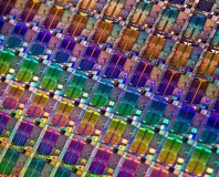
Scientists from the University of Cambridge have created what they claim is the world's first true three-dimensional microchip using spintronic technology.
While devices such as Intel's tri-gate transistors, as found in the Ivy Bridge family of processors, and associated FinFETs are often billed as being three dimensional, in truth their interconnections are as two-dimensionally planar as anything that has come before. The prototype device created at Cambridge, however, is truly 3D in its operation. 'Today’s chips are like bungalows – everything happens on the same floor,' explained Reinhoud Lavrijsen, one of the authors of the paper describing the research, in a news posting. 'We’ve created the stairways allowing information to pass between floors.'
The prototype device ditches traditional electronics for spintronics, which exploit the magnetic spin of an electron rather than its charge. One of the technologies tipped to replace traditional dynamic RAM (DRAM) in the near future, the spintronic chip was created from layers of cobalt, platinum and ruthenium atoms deposited on a silicon chip in a process that goes by the not-terribly-scientific-sounding name of 'sputtering.' The data is stored on the cobalt and platinum atoms, while the ruthenium acts as a network between layers.
Reading the data back with a laser - the first hint that the group's work is currently only lab-ready, rather than commercially exploitable - the team saw the data climb up each layer from the bottom of the chip to the top as a magnetic field was toggled. Dubbed a 'spintronic staircase,' the system proved that a three-dimensional chip was viable.
Not to be confused with chip-stacking technologies, like the through-silicon vias used in Micron's Hybrid Memory Cubes, the research promises to create truly three-dimensional arrays on a single silicon wafer. 'Each step on our spintronic staircase is only a few atoms high,' boasted Russel Cowburn, lead researcher of the study and professor at the University of Cambridge's Department of Physics. 'This is a great example of the power of advanced materials science. Traditionally, we would use a series of electronic transistors to move data like this. We’ve been able to achieve the same effect just by combining different basic elements such as cobalt, platinum and ruthenium. This is the 21st century way of building things – harnessing the basic power of elements and materials to give built-in functionality.'
The team hopes that its research could lead to high-performance and high-density spintronic memory chips, but it's clear that work still needs to be done on bringing the technology to market.


MSI MPG Velox 100R Chassis Review
October 14 2021 | 15:04

Want to comment? Please log in.