Intel has announced investment in ASML Holding, a company which produces semiconductor manufacturing equipment, to the tune of €3.3 billion as it looks to move its manufacturing process to 450mm wafers.
In addition to cash investment in the firm of €1.7 billion - for which Intel gets an immediate 10 per cent stake, and commits to buy a further 5 per cent in ASML's next share issue - the company has committed €829 million to extend ASML's research and development in the areas of 450mm lithography and extreme ultra-violet (EUV) lithography.
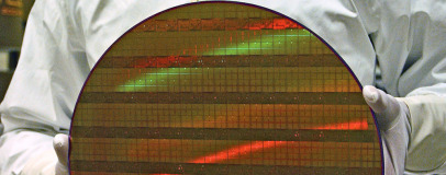
First, the 450mm deal: over the next five years, Intel will provide ASML with €553 million to research and develop tools and techniques for the move to 450mm wafer sizes, along with the €1.7 billion investment for 10 per cent of the firm's equity. It's a move Intel, and its rivals in the semiconductor industry, need to make: larger wafers mean more efficient production processes, and a serious dip in manufacturing costs and environmental impact.
The next part of the deal sees Intel earmarking a further €276 million over the next five years for research into extreme ultra-violet (EUV) lithography, which uses a 13.5nm wavelength light source to transfer the pattern of the component's photomask onto the wafer's photoresist substrate ready for engraving or deposition. EUV, however, is far from a simple process: unlike traditional optical or UV photolithography, EUV lithography needs to take place in a vacuum - meaning ASML needs to do some serious work in producing reliable, affordable machinery.
The complexity of EUV has led to a certain slowdown in development: most 20nm-class components are produced using traditional immersion lithography techniques and a technique known as multiple patterning which increases feature density. Currently, the state of the art in EUV lithography is around 28nm; with Intel's investment, EUV could become the standard for sub-20nm components
To help things along, Intel will be providing a further €838 million incrementally to purchase an additional five per cent of ASML, bringing its total ownership of the company to 15 per cent. It won't be alone: a further 10 per cent is to be offered to other investors on a similar basis, potentially allowing Intel's rivals similar access to ASML's research and development division.
'Productivity improvements driven by enhanced wafer manufacturing technologies, especially larger silicon wafers and enhanced lithography technologies with EUV are direct enablers of Moore's Law, which delivers significant economic benefits to consumers,' claimed Brian Krzanich, Intel senior vice president and chief operating officer, of the deal. 'The transition from one wafer size to the next has historically delivered a 30 to 40 percent reduction in die cost and we expect the shift from today's standard 300-mm wafers to larger 450mm wafers to offer similar benefits. The faster we do this, the sooner we can gain the benefit of productivity improvements, which creates tremendous value for customers and shareholders.'
In addition to cash investment in the firm of €1.7 billion - for which Intel gets an immediate 10 per cent stake, and commits to buy a further 5 per cent in ASML's next share issue - the company has committed €829 million to extend ASML's research and development in the areas of 450mm lithography and extreme ultra-violet (EUV) lithography.
First, the 450mm deal: over the next five years, Intel will provide ASML with €553 million to research and develop tools and techniques for the move to 450mm wafer sizes, along with the €1.7 billion investment for 10 per cent of the firm's equity. It's a move Intel, and its rivals in the semiconductor industry, need to make: larger wafers mean more efficient production processes, and a serious dip in manufacturing costs and environmental impact.
The next part of the deal sees Intel earmarking a further €276 million over the next five years for research into extreme ultra-violet (EUV) lithography, which uses a 13.5nm wavelength light source to transfer the pattern of the component's photomask onto the wafer's photoresist substrate ready for engraving or deposition. EUV, however, is far from a simple process: unlike traditional optical or UV photolithography, EUV lithography needs to take place in a vacuum - meaning ASML needs to do some serious work in producing reliable, affordable machinery.
The complexity of EUV has led to a certain slowdown in development: most 20nm-class components are produced using traditional immersion lithography techniques and a technique known as multiple patterning which increases feature density. Currently, the state of the art in EUV lithography is around 28nm; with Intel's investment, EUV could become the standard for sub-20nm components
To help things along, Intel will be providing a further €838 million incrementally to purchase an additional five per cent of ASML, bringing its total ownership of the company to 15 per cent. It won't be alone: a further 10 per cent is to be offered to other investors on a similar basis, potentially allowing Intel's rivals similar access to ASML's research and development division.
'Productivity improvements driven by enhanced wafer manufacturing technologies, especially larger silicon wafers and enhanced lithography technologies with EUV are direct enablers of Moore's Law, which delivers significant economic benefits to consumers,' claimed Brian Krzanich, Intel senior vice president and chief operating officer, of the deal. 'The transition from one wafer size to the next has historically delivered a 30 to 40 percent reduction in die cost and we expect the shift from today's standard 300-mm wafers to larger 450mm wafers to offer similar benefits. The faster we do this, the sooner we can gain the benefit of productivity improvements, which creates tremendous value for customers and shareholders.'
RELATED ARTICLES


MSI MPG Velox 100R Chassis Review
October 14 2021 | 15:04

Want to comment? Please log in.