Global Foundries announces ambitious expansion plans
June 2, 2010 | 02:32
Companies: #global-foundries #tsmc
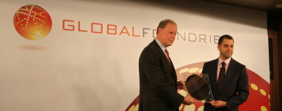
COMPUTEX 2010 Global Foundries, the manufacturing company formed when AMD decided to become purely a chip design outfit, this morning announced an ambitious program of upgrades to its factories.
It will increase both the scale and complexity of its fabrication plants (fabs for short), meaning companies which don't own their own plants - increasingly common in the high-tech world - have access to better and better manufacturing processes for their wares.
With a current global capacity of 110,000 300mm wafers per month split between Fab 1 in Germany and Fab 7 in Singapore, the addition of the new Fab 8 in New York will bring an extra 42,000 wafers when it’s finished in 2012. This will further increase with the construction of an additional cleanroom Fab 1 Germany making it the largest in Europe – something Global Foundries classes as its ‘Gigalab’. The extra 110,000 sq foot of space in clean room adds 25 per cent capacity, increasing output from 60,000 to 80,000 wafers a month by mid-2011. The Dresden lab is still focused on 40 and 45nm process manufacturing, moving to 28nm by next year. The advantage of extra production volume means that Global Foundaries can learn faster to improve yields.
Despite the fact it’s not even finished yet, expansion of Fab 8 in New York will also take place in “phase 2” of its construction, adding 40% more cleanroom space and focusing on 28nm production, before moving to 22/20nm and below, ultimately increasing production output to 60,000 wafers a month by 2013.
At its Computex press conference, Global Foundries stated that its new High-k metal gate techniques on 32nm and 28nm are in the early introduction phase, but this process was also “design compatible” with 45/40nm production and accounts for a 10-15 per cent die size reduction and transistor performance equal to Intel (although it's arguably coming two years behind Intel).
Global Foundries continues to use volume immersion lithography and double patterning with 32nm and will move to Extreme Ultra Violet (EUV) in 2011 with mask and resist technique.
How do you feel Global Foundaries stacks up against its largest competitor, TSMC? Can either catch Intel’s current manufacturing lead? Let us know your thoughts, in the forums.
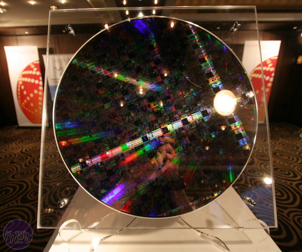
Global Foundaries 28nm 300mm test wafer was on show
It will increase both the scale and complexity of its fabrication plants (fabs for short), meaning companies which don't own their own plants - increasingly common in the high-tech world - have access to better and better manufacturing processes for their wares.
With a current global capacity of 110,000 300mm wafers per month split between Fab 1 in Germany and Fab 7 in Singapore, the addition of the new Fab 8 in New York will bring an extra 42,000 wafers when it’s finished in 2012. This will further increase with the construction of an additional cleanroom Fab 1 Germany making it the largest in Europe – something Global Foundries classes as its ‘Gigalab’. The extra 110,000 sq foot of space in clean room adds 25 per cent capacity, increasing output from 60,000 to 80,000 wafers a month by mid-2011. The Dresden lab is still focused on 40 and 45nm process manufacturing, moving to 28nm by next year. The advantage of extra production volume means that Global Foundaries can learn faster to improve yields.
Despite the fact it’s not even finished yet, expansion of Fab 8 in New York will also take place in “phase 2” of its construction, adding 40% more cleanroom space and focusing on 28nm production, before moving to 22/20nm and below, ultimately increasing production output to 60,000 wafers a month by 2013.
At its Computex press conference, Global Foundries stated that its new High-k metal gate techniques on 32nm and 28nm are in the early introduction phase, but this process was also “design compatible” with 45/40nm production and accounts for a 10-15 per cent die size reduction and transistor performance equal to Intel (although it's arguably coming two years behind Intel).
Global Foundries continues to use volume immersion lithography and double patterning with 32nm and will move to Extreme Ultra Violet (EUV) in 2011 with mask and resist technique.
How do you feel Global Foundaries stacks up against its largest competitor, TSMC? Can either catch Intel’s current manufacturing lead? Let us know your thoughts, in the forums.
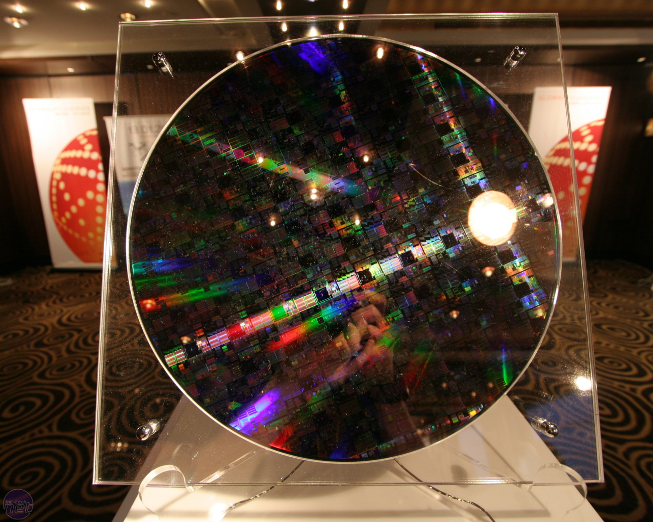
Global Foundaries 28nm 300mm test wafer was on show
RELATED ARTICLES


MSI MPG Velox 100R Chassis Review
October 14 2021 | 15:04

Want to comment? Please log in.