IBM Technology Alliance reveals 28nm chip plans
April 17, 2009 | 14:53
Companies: #amd #arm #globalfoundries #ibm #samsung

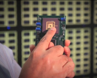
Intel only revealed its 32nm technology a couple of months ago, but IBM has now revealed that it’s already in the process of developing the technology for 28nm transistors. Yesterday, the company announced that the partners in the IBM Technology Alliance have now defined the standards for the 28nm technology, which the companies in the alliance will be jointly developing.
The IBM Technology Alliance features many key chip makers, including Samsung Electronics, Chartered Semiconductor Manufacturing, Infineon Technologies and STMicroelectronics. Perhaps more importantly, however, the alliance now also includes AMD’s former fabrication business, GlobalFoundries, which will now also be taking part in the development of 28nm chips.
As with Intel and IBM’s current 32nm chip designs, the 28nm chips will use low-leakage high-k metal gate technology, and IBM says that its early tests indicate that the 28nm chips can provide up to a 40 percent performance improvement over 45nm chips, with a 20 percent reduction in power consumption. The size of the chips will also be impressive; IBM claims that the technology will enable the production of SRAM cells that measure just 0.12 square microns.
A major target market for the technology is mobile Internet devices, and IBM says that the 28nm high-k metal gate technology will enable lower power consumption in standby mode, while also extending battery life.
IBM’s plans for 28nm technology were also mentioned in September 2008, when the Common Platform alliance (Chartered Semiconductor Manufacturing and Samsung Electronics) announced that it had teamed up with ARM to design a system-on-chip platform that used both 32nm and 28nm technology. The platform’s 32nm ARM Cortex processor was revealed at the Mobile World Congress in February.
IBM’s vice president of its Semiconductor Research and Development Center, Gary Patton, said that "Through this collaboration, IBM and its alliance partners are helping to accelerate development of next-generation technology to achieve high-performance, energy-efficient chips at the 28nm process level, maintaining our focus on technology leadership for our clients and partners."
The IBM Technology Alliance expects the first 28nm chips to go into “early risk” production in the second half of 2010, and evaluation kits have been made available to the chip market since March 2009.
Are you impressed by the IBM Technology Alliance’s plans for 28nm chips, and how will the technology affect the silicon industry? Let us know your thoughts in the forums.
RELATED ARTICLES


MSI MPG Velox 100R Chassis Review
October 14 2021 | 15:04

Want to comment? Please log in.