
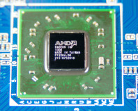
Inside AMD's 890GX and SB850 chipset
Manufacturer: AMDAMD's chipsets have been getting better and better in recent years - mostly thanks to the acquisition of ATI - and its latest 890GX (and more notably, the SB850 southbridge it's paired with), is actually ahead of Intel in terms of features.
It's still a two chip product rather than an all-in-one, but there are benefits to this. For starters, it means both cores can be developed separately and designed quicker, it spreads the heat generated over more board surface area, and also the new southbridge can be paired with other future 8-series chipsets: we're already anticipating the replacement for the aging 790FX and 785G in time as well. However the obvious downsides is that two chips take more physical space and it's more expensive to fabricate two parts than just one, plus it requires more high-bandwidth motherboard tracing to cope with the latest features such as USB 3 and SATA 6Gbps.
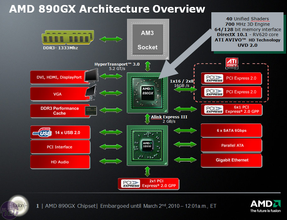
The basic architecture is pretty much identical as before: the 890GX northbridge connects to both the AM3 socket via a 5.2GT/sec HyperTransport 3.0 link, and then to the SB850 Southbridge by the same x4 PCI-Express link that is now branded as "ALink Express III" at 2GB/s.
Click to enlarge
AMD's 890GX itself is an evolutionary product and can be thought of as a 785G updated to 790GX spec. The 890GX is identical to the 790GX in its support for a single x16 PCI-Express 2.0 lane that can be split into two x8 PCI-E 2.0 for Crossfire, and there's still six extra x1 PCI-E 2.0 connections for additional motherboard slots or features. Powering the latter x1 slot from the northbridge offloads a potential bandwidth demands on the Alink Express III bus, had these been bolted to the southbridge instead.
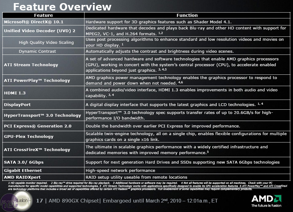
Integrated graphics is where the 785G comparison comes in: the 890GX uses the same RV620 core, based on the Radeon 3000-series, rebranded to 4000-series thanks to featuring version 2.0 of UVD. The graphics core has the same 40 (8 blocks of 5) unified shaders, 64-128-bit memory interface via the CPU and is DirectX 10.1 compatible. Where the 785G's Radeon HD4200 had a core clock of 500MHz, the 890GX's Radeon HD 4290 pushes this up to 700MHz. That said, almost every 785G could overclock that far and beyond anyway. In our tests overclocking never made a difference and while there's still the same DDR3 'Sideport' cache memory option, that didn't help the FPS either.
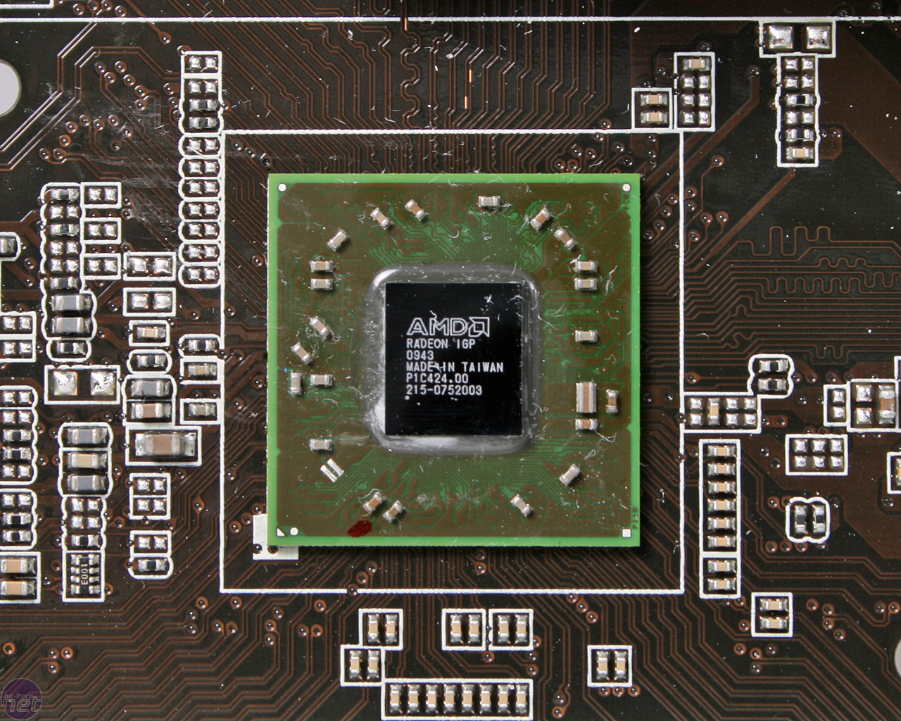

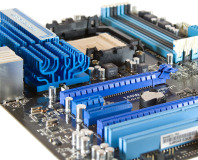
Left, the 890GX northbridge. Right, the SB850 southbridge. Click to enlarge
The display outputs are a familiar DVI, D-Sub, HDMI and DisplayPort, but dual digital outputs are not possible. UVD 2.0 is a couple of versions behind the latest discreet Radeons, which uses UVD 2.2 that includes the HDMI 1.3a spec for 7.1 channel HD audio pass-through. Serious HTPC guys will have to look to the Radeon HD 5450 - but realistically speaking, UVD 2.0 covers everything the vast majority of people (i.e. those without 7.1 surround sound and expensive amps) want from a HTPC, so consider we're missing a 'nice to have' rather than an essential part.
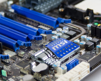
The SB850 southbridge is considerably more interesting. For starters AMD has integrated six of the latest SATA 6Gbps ports into it, meaning future support for the latest SSDs and hard drives that have already started with Seagate’s Barracuda XT and Micron's RealSSD C300. It's also the first time we'll be able to try RAID 5 with SATA 6Gbps; RAID 0, 1, and 10 are also featured.

Click to enlarge
AMD still includes support for a single IDE port to be implemented at a manufacturer’s discretion, physical layer Gigabit Ethernet, a standard HD audio connection and two further x1 PCI-E 2.0 lanes. That's proper 2.0 bandwidth at 500MB/s, not Intel's '2.0' x1 lanes on its PCH's that only offer 250MB/s. Finally USB has been updated from 12 to 14 ports, but doesn't feature USB 3 support.
One notable omission is Advanced Clock Calibration, or ACC. Primed by AMD as the key to performance unlocking on the original Phenoms, and later slightly used by Phenom IIs, its biggest benefit was allowing core unlocking on Phenom II X2 and X3 parts to make them full X4 quad cores. This, unfortunately, is no more.
Or is it? At the time of writing Gigabyte and MSI told us the new chipset does not (and alluded to will not) have the unlock function, however Asus' sent us its latest M4A89GTD Pro/USB and claimed it still could. We successfully tested on a Phenom II X3 720 Black Edition and it unlocked the fourth core, so clearly it's still possible, although whether it just takes a BIOS hack or some actual PCB engineering time, we're not sure. We'd imagine that despite the resounding "no" on the unlocking front right now, more and more companies will follow Asus' lead and engineer it in. It's arguably a more important factor than USB 3 or SATA 6Gbps, because of its tangible value-add.
If you're interested to see how the 890GX and SB850 fare, check out our full review of the Asus M4A89GTD Pro/USB.
Click to enlarge
RELATED ARTICLES


MSI MPG Velox 100R Chassis Review
October 14 2021 | 15:04

Want to comment? Please log in.