Intel has given some high level details of a new technology called Foveros, a 3D packaging technology that will make a debut in products next year and which will allow complex and different logic chips to be stacked directly on top of each other.
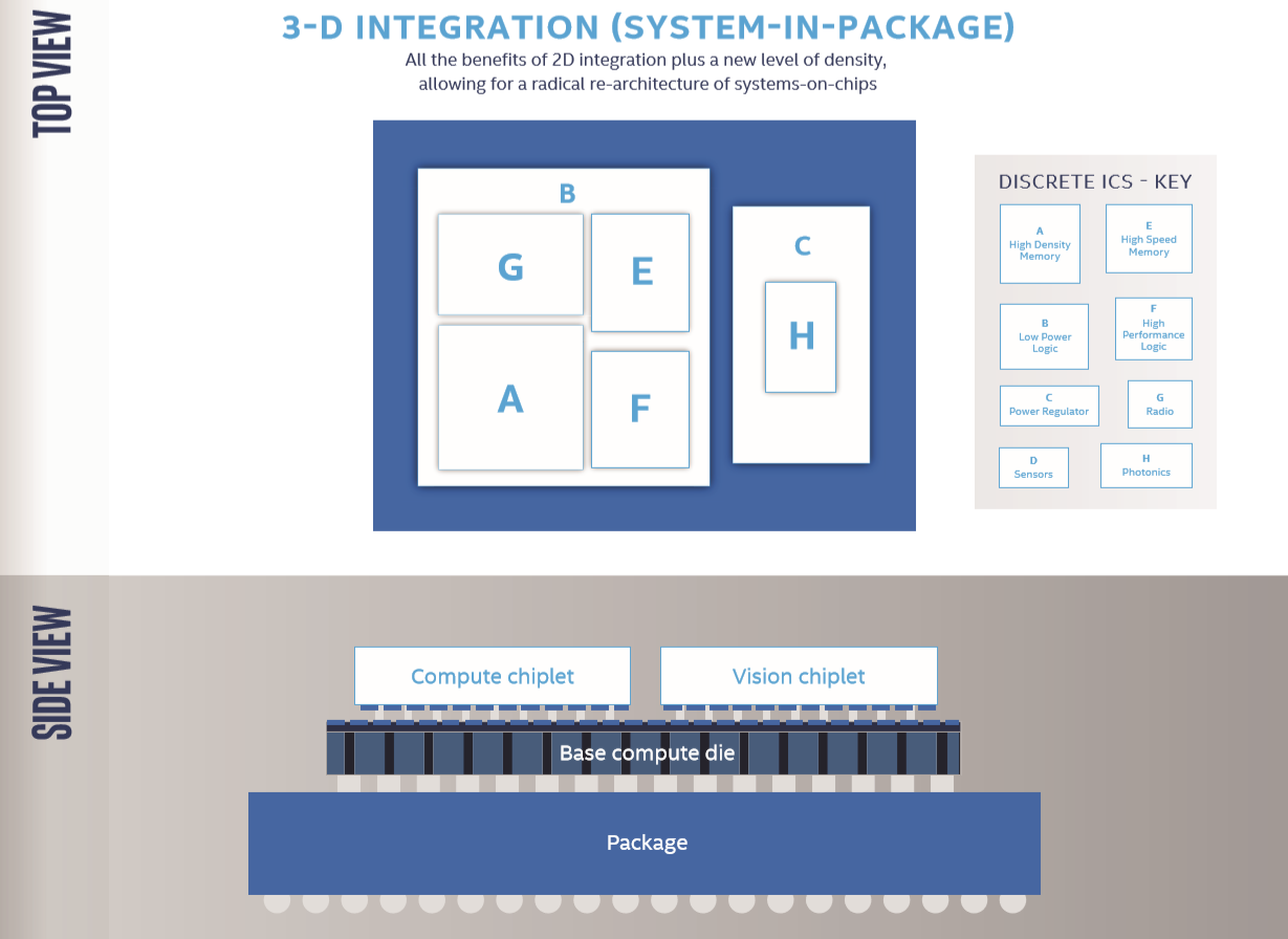
As a producer of a huge variety of different integrated circuits (ICs) with many different functions as well as different performance/power/cost balancing needs, Intel knows all too well that no single process node is optimal for all of them. As such, when it comes to system-on-chip (SoC) design, the case for heterogeneous systems, where ICs are manufactured discretely and later combined onto a single package (system-in-package, or SiP), is strong. Instead of a monolithic design, where all parts of a given SoC (e.g. CPU cores, comms, I/O, etc.) are manufactured on the same node and combined on a single die, the heterogeneous approach allows each IC to be manufactured on the process that is optimal for it, and it also ensures maximum flexibility in design by allowing customers to mix and match ICs for specific purposes. Further, it avoids yield issues that come from increasing die size and complexity.
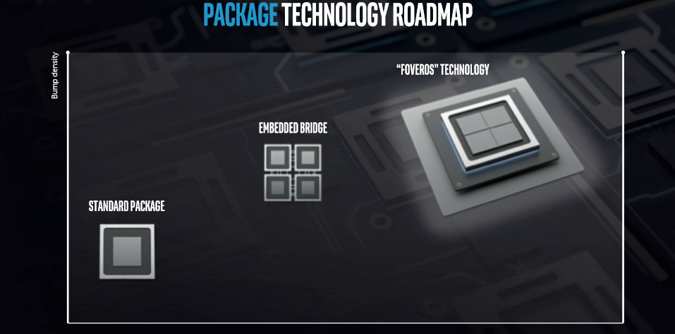
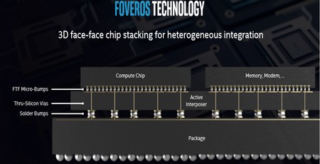
Of course, you then need an efficient way to connect the individual ICs, and Intel made good progress in this regard last year with its Embedded Multi-die Interconnect Bridge (EMIB). However, EMIB is very much a 2D solution; the edge-to-edge connectivity necessitates that individual dies be placed next to each other.
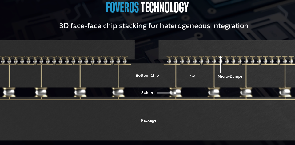
What Foveros cleverly brings to the table is 3D stacking of discrete ICs, effectively enabling logic-on-logic integration. Face-to-face micro-bumps connect one IC to another, while through-silicon vias (TSVs) are then used to connect to the package below directly through the bottom die. This turns the lowest layer into an active interposer (as opposed to the traditional passive interposer layer which is used when connecting HBM memory to a GPU, for example). According to Intel, Foveros is both high in bandwidth and low in power demands.
The idea is to combine the space saving benefits of 3D stacking with logic-logic integration. Intel gives the example of using a low-cost process (22FFL) for a base SoC/IO die with a dedicated compute model produced on the more complex and more expensive I(but more optimal) 10nm node stacked on top, and then combined with more traditional product-on-product (PoP) memory.
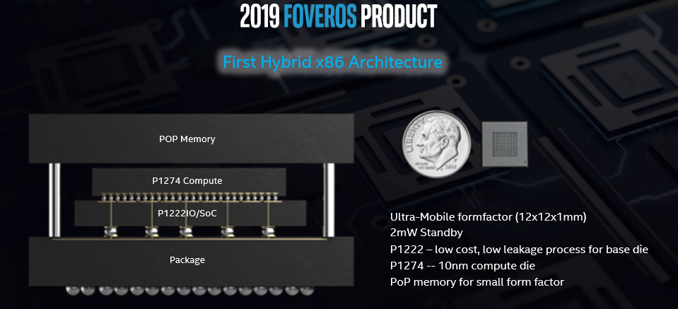
In fact, 2019 will see Foveros launch with a product just like this and achieving an ultra-mobile form factor of just 12x12mm. A range of additional products are expected to roll out in the second half of 2019, and Intel plans to leverage Foveros across a wide range of its IP including graphics, CPU, server, network SoC, and more.


MSI MPG Velox 100R Chassis Review
October 14 2021 | 15:04

Want to comment? Please log in.