Samsung boasts of 12-layer 3D-TSV breakthrough
October 7, 2019 | 10:23
Companies: #samsung-electronics
Samsung Electronics has announced the development of what it claims is the semiconductor industry's first 12-layer through-silicon via (TSV) technology, allowing it to stack 12 DRAM dies in a single package.
The march of Moore's Law, the observation turned golden rule by Intel co-founder Gordon Moore that the number of transistors on a leading-edge part trends towards a doubling every 18 months, brings with it the need to pack ever-more components into ever-shrinking spaces - lest you end up with CPUs the size of football pitches. While shrinking the size of said components is one approach, it brings with it a range of difficulties as various laws of physics make themselves known as feature sizes drop; an alternative is to stack multiple dies on top of each other, much like building a skyscraper boosts the number of people you can house in a given square footage.
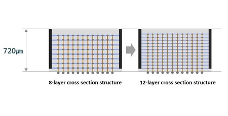
Samsung Electronics has announced a new milestone in 3D chip packaging using through-silicon via (TSV) technology, which places holes in each die to allow electrical interconnects between higher dies and lower dies: 12 layers, which the company says required the creation of 60,000 TSV holes each one-twentieth the thickness of a human hair.
'Packaging technology that secures all of the intricacies of ultra-performance memory is becoming tremendously important, with the wide variety of new-age applications, such as artificial intelligence (AI) and High Power Computing (HPC),' says Hong-Joo Baek, executive vice president of test and system package at Samsung Electronics. 'As Moore's law scaling reaches its limit, the role of 3D-TSV technology is expected to become even more critical. We want to be at the forefront of this state-of-the-art chip packaging technology.'
The 12-layer 3D-TSV parts build on their eight-layer predecessors, used by Samsung to produce High-Bandwidth Memory 2 (HBM2) components, and impressive retain the same 720㎛ thickness. Despite adding four more layers, Samsung is also claiming that the new technique reduces data transmission time between layers to boost speed while lowering power consumption - though, someone disingenuously, is making the comparison between its 3D-TSV technology and rival parts which use wire bonding on the edges of each die. Capacity is also boosted, naturally, with Samsung claiming that the 8GB HBM2 parts it produces at the moment, based on eight 8Gb layers, will be succeeded by a 24GB part based on 12 layers of 16Gb apiece.
Samsung has not yet offered a release date for the first parts to use the 12-layer 3D-TSV technology.


MSI MPG Velox 100R Chassis Review
October 14 2021 | 15:04

Want to comment? Please log in.