Toshiba unveils 1TB TSV-packing BiCS flash chips
July 11, 2017 | 11:34
Companies: #toshiba #toshiba-memory-corporation
Toshiba has announced what it claims to be the world's first three-dimensional triple-level cell (TLC) flash memory chip to use through-silicon via (TSV) technology, allowing for a boost in capacity to 1TB in a single stacked package.
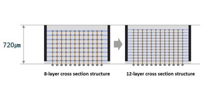
Toshiba's latest breakthrough in solid-state storage builds on two separate projects previously announced: the BiCS4 96-layer 3D flash memory technology it developed with joint venture partner Western Digital, and a 16-layer stacked NAND module it developed back in 2015. At the time, the company claimed the use of through-silicon vias (TSVs) - tunnels created through the layers of silicon themselves, allowing direct connectivity between layers without the usual wire bonding - allowed for 1Gb/s data rates, a 50 percent reduction in power usage, and up to 256GB in a 16-layer stacked BGA-152 module measuring 14mm by 18mm and 1.9mm tall.
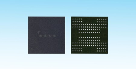
Its latest prototype design uses the same 16-layer silicon encased in a BGA-152 package measuring 14mm by 18mm but at a slightly reduced 1.85mm tall, but the switch to use triple-level cell (TLC) BiCS flash has resulted in a significant boost in capacity from 256GB to a whopping 1TB - in, remember, a single chip smaller than a First Class stamp. According to Toshiba, the move to BiCS hasn't left any of the advantages of TSV technology by the wayside: Like its lower-capacity predecessor both the 512GB eight-layer and 1TB 16-layer prototypes offer twice the energy efficiency compared to the same modules with traditional wire bonding.
The company has indicated it began quietly shipping prototype modules to hardware partners in June and expects the first product samples to be released in the second half of the year. The company is, however, currently silent on retail availability of drives based around the technology.


MSI MPG Velox 100R Chassis Review
October 14 2021 | 15:04

Want to comment? Please log in.