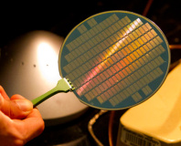
Researchers create 20nm '4-D' InGaAs transistors
December 7, 2012 | 10:44
Companies: #purdue-university

Researchers have revealed a new design of transistor which extends the concept of three-dimensional circuits yet further - and, topically given the time of year, is shaped vaguely enough like a Christmas tree for the fir to get a nod in the official press release.
Developed by a team comprised of researchers from Purdue and Harvard universities, the new transistor design is constructed from indium-gallium-arsenide rather than silicon. Its design uses three nanowires, each progressively smaller, providing a cross-section which Purdue claims looks like a Christmas tree. A bit. If you squint.
The team's research represents an extension of the current interest in three-dimensional transistor arrays, designed to offer improved performance over traditional planar transistor layouts. The most famous of these is Intel's Tri-Gate Transistor, found in the latest Ivy Bridge processor family, while other manufacturers are working on their own implementations. The Christmas-tree version, however, goes further - so much so, it's breaking the laws of geometry.
'It's a preview of things to come in the semiconductor industry. A one-story house can hold so many people, but more floors, more people, and it's the same thing with transistors,' explained Peide 'Peter' Ye, professor of electrical and computing engineering at Purdue University, of his team's work. 'Stacking them results in more current and much faster operation for high-speed computing. This adds a whole new dimension, so I call them 4-D.'
Ignoring Ye's overenthusiastic application of a supposed fourth dimension, the team's work seems like a sound basis for the continued shrinking of process size in the semiconductor industry: below 22nm, planar transistor layouts run into severe problems while a three-dimensional layout using a non-silicon material such as indium-gallium-arsenide should be suitable for sub-10nm parts.
To help drive this process of increasing transistor density, the team also looked at a new composite insulator to reduce current leakage - a serious problem at small process sizes. Using a dialetric layer just 4.5nm thick, constructed from lanthanum aluminate with a half-nanometre layer of aluminium oxide on top, the team created the first indium-gallium-arsenide transistors with 20nm gates - a good indication that the work will be suitable for commercial exploitation in the future.
How far in the future is, of course, something neither university is discussing, and the team is even refusing to release an image of the supposed Christmas-tree shaped prototype device until the work is presented at the International Electron Devices Meeting in San Francisco this weekend.

MSI MPG Velox 100R Chassis Review
October 14 2021 | 15:04


Want to comment? Please log in.