Researchers point to nanoscale cooling breakthrough
April 22, 2015 | 12:10
Companies: #research #university-of-colorado
A discovery made by researchers on cooling nanoscale devices could lead to a boost for Moore's Law, celebrating its 50th anniversary this week, and the future of semiconductors in general.
Moore's Law, the report by Intel co-founder Gordon Moore that the number of transistors on an integrated circuit tends to double every 18 months, turned 50 this week. Originally a simple observation of trends, the semiconductor industry has taken Moore's Law to heart and it has become a do-or-die imperative: the number of transistors it's possible to fit on a single integrated circuit must double every 18 months, give or take. For years, that has led to decreasing manufacturing node sizes - but Intel recent stumbled as it attempted to produce 14nm parts, delaying the launch and casting doubt on whether it will hit its roadmap for future process node shrinkages.
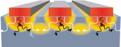
There are several problems with making everything on an integrated circuit smaller, and one of the biggest is heat: the smaller the transistors are and the closer together they are packed, the more heat the IC generates and the harder it becomes to cool. Researchers have, however, made a breakthrough discovery which may help the semiconductor industry continue its slavish adherence to Moore's Law for a few years longer: nanoscale heat sources cool better when placed closer together, rather than farther apart.
Described by the researchers, a joint team at the University of Colorado and the Lawrence Berkeley National Laboratory, as 'counter-intuitive,' the discovery suggests new approaches for cooling ever-smaller and tightly-packed semiconductors, as well as having implications for everything from solar panels through to thermoelectric devices.
Cooling in nanoscale devices is, the team explains, determined by a number of factors including the length scales of the heat sources and the distribution of carrier mean free paths in the material. Traditionally, it has been thought that the most efficient cooling comes from having heat sources larger than the free paths - allowing each source access to multiple free paths for cooling. The team's research shows that the opposite is the case: having heat sources smaller than the free paths leads to increased cooling efficiency. In other words: nanoscale devices cool better when more tightly packed than when widely separated.
This finding, proved experimentally, turns traditional thinking on its head and could lead to a revolution in semiconductor design - but it has a long way to go as it moves from the lab to the fab, and thus far no semiconductor companies have come forward to say they are adopting or even investigating the team's findings.
The work can be read in full in the Proceedings of the National Academy of Sciences of the United States of America journal, Volume 112 Number 16.
Moore's Law, the report by Intel co-founder Gordon Moore that the number of transistors on an integrated circuit tends to double every 18 months, turned 50 this week. Originally a simple observation of trends, the semiconductor industry has taken Moore's Law to heart and it has become a do-or-die imperative: the number of transistors it's possible to fit on a single integrated circuit must double every 18 months, give or take. For years, that has led to decreasing manufacturing node sizes - but Intel recent stumbled as it attempted to produce 14nm parts, delaying the launch and casting doubt on whether it will hit its roadmap for future process node shrinkages.
There are several problems with making everything on an integrated circuit smaller, and one of the biggest is heat: the smaller the transistors are and the closer together they are packed, the more heat the IC generates and the harder it becomes to cool. Researchers have, however, made a breakthrough discovery which may help the semiconductor industry continue its slavish adherence to Moore's Law for a few years longer: nanoscale heat sources cool better when placed closer together, rather than farther apart.
Described by the researchers, a joint team at the University of Colorado and the Lawrence Berkeley National Laboratory, as 'counter-intuitive,' the discovery suggests new approaches for cooling ever-smaller and tightly-packed semiconductors, as well as having implications for everything from solar panels through to thermoelectric devices.
Cooling in nanoscale devices is, the team explains, determined by a number of factors including the length scales of the heat sources and the distribution of carrier mean free paths in the material. Traditionally, it has been thought that the most efficient cooling comes from having heat sources larger than the free paths - allowing each source access to multiple free paths for cooling. The team's research shows that the opposite is the case: having heat sources smaller than the free paths leads to increased cooling efficiency. In other words: nanoscale devices cool better when more tightly packed than when widely separated.
This finding, proved experimentally, turns traditional thinking on its head and could lead to a revolution in semiconductor design - but it has a long way to go as it moves from the lab to the fab, and thus far no semiconductor companies have come forward to say they are adopting or even investigating the team's findings.
The work can be read in full in the Proceedings of the National Academy of Sciences of the United States of America journal, Volume 112 Number 16.


MSI MPG Velox 100R Chassis Review
October 14 2021 | 15:04

Want to comment? Please log in.