Chipworks has published an initial analysis of the semi-custom AMD accelerated processing unit (APU) that powers Sony's PlayStation 4, following the console's North American launch.
The PS4 is a departure from the company's traditional approach: where the original PlayStation, the PS2 and the PS3 all used somewhat esoteric instruction set architectures - MIPS in the first two iterations and the hybrid Power architecture known as Cell in the third - the company's forth console generation uses the familiar 64-bit x86 architecture. As before, however, the chip at the heart of the console isn't an off-the-shelf component but a semi-custom design tweaked to Sony's requirements in unspecified ways by manufacturer AMD.
Now, semiconductor expert Chipworks has offered glimpse of just what AMD has put into the CXD90026G chip at the heart of Sony's next-generation console - and in doing so offered hints as to what to expect from Microsoft's rival Xbox One when it launches on Friday.
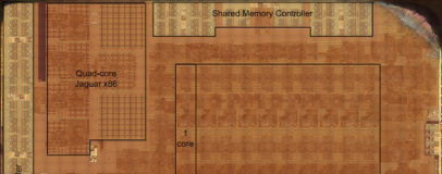
According to the company's initial technical analysis, the PS4's CXD90026G processor features a die size of 348mm² - a serious increase over the combined 228mm² die size of the CPU and GPU found in the PS3. Imaging of the chip shows the expected eight Jaguar processing cores present and correct, split into two quad-core blocks squished into the left-hand edge of the die. A surprise, however, is a total of 20 Graphics Core Next Compute Units for a total of 1,280 shaders - more than the expected 18 blocks totalling 1,152 shaders.
Before readers with PS4 pre-orders get too excited, however, it appears that two of the 20 GPU units are inactive - suggesting that the extra blocks are there to improve yield at manufacturing, allowing for up to 10 per cent of the GPU components to fail without affecting the final performance of the chip. Should yields improve, however, it's possible Sony could release an updated PS4 with all 20 GPU units activated - although whether it would split its customer base in this fashion is questionable, even if the extra power is only used to smooth out performance slightly.
The floor plan of the die also reveals memory controllers located on three edges, matching the layout of the motherboard which places GDDR5 memory modules at the left, top and bottom of the APU. The remaining edge, at the right-hand side of the chip, is used for communication to components on the remainder of the motherboard.
The company's analysis also suggests that the twelve-layer design is manufactured by AMD using Taiwan Semiconductor (TSMC) High-K Metal Gate (HKMG) process at a 28nm node - and concludes it's likely exactly the same process AMD uses for its latest Radeon GPUs.
While Chipworks' analysis reveals much about Sony's custom APU, the real secrets will likely only show themselves when the rival Xbox One - with its own semi-custom eight-core AMD APU - launches on Friday and offers the opportunity for the same analysis and a direct comparison between the design of the two parts.
The PS4 is a departure from the company's traditional approach: where the original PlayStation, the PS2 and the PS3 all used somewhat esoteric instruction set architectures - MIPS in the first two iterations and the hybrid Power architecture known as Cell in the third - the company's forth console generation uses the familiar 64-bit x86 architecture. As before, however, the chip at the heart of the console isn't an off-the-shelf component but a semi-custom design tweaked to Sony's requirements in unspecified ways by manufacturer AMD.
Now, semiconductor expert Chipworks has offered glimpse of just what AMD has put into the CXD90026G chip at the heart of Sony's next-generation console - and in doing so offered hints as to what to expect from Microsoft's rival Xbox One when it launches on Friday.
According to the company's initial technical analysis, the PS4's CXD90026G processor features a die size of 348mm² - a serious increase over the combined 228mm² die size of the CPU and GPU found in the PS3. Imaging of the chip shows the expected eight Jaguar processing cores present and correct, split into two quad-core blocks squished into the left-hand edge of the die. A surprise, however, is a total of 20 Graphics Core Next Compute Units for a total of 1,280 shaders - more than the expected 18 blocks totalling 1,152 shaders.
Before readers with PS4 pre-orders get too excited, however, it appears that two of the 20 GPU units are inactive - suggesting that the extra blocks are there to improve yield at manufacturing, allowing for up to 10 per cent of the GPU components to fail without affecting the final performance of the chip. Should yields improve, however, it's possible Sony could release an updated PS4 with all 20 GPU units activated - although whether it would split its customer base in this fashion is questionable, even if the extra power is only used to smooth out performance slightly.
The floor plan of the die also reveals memory controllers located on three edges, matching the layout of the motherboard which places GDDR5 memory modules at the left, top and bottom of the APU. The remaining edge, at the right-hand side of the chip, is used for communication to components on the remainder of the motherboard.
The company's analysis also suggests that the twelve-layer design is manufactured by AMD using Taiwan Semiconductor (TSMC) High-K Metal Gate (HKMG) process at a 28nm node - and concludes it's likely exactly the same process AMD uses for its latest Radeon GPUs.
While Chipworks' analysis reveals much about Sony's custom APU, the real secrets will likely only show themselves when the rival Xbox One - with its own semi-custom eight-core AMD APU - launches on Friday and offers the opportunity for the same analysis and a direct comparison between the design of the two parts.


MSI MPG Velox 100R Chassis Review
October 14 2021 | 15:04

Want to comment? Please log in.