Samsung tapes out first 14nm FinFET-based parts
December 21, 2012 | 10:38
Companies: #arm #common-platform #globalfoundries #samsung
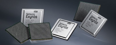
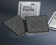
Samsung has announced the successful taping-out of the its first FinFET devices based on a 14nm lithographic process, in the continued drive to boost performance of mobile devices while dropping power draw.
FinFET - fin-based three-dimensional field effect transistors - are designed to improve performance and reduce current leakage at smaller process sizes by extending the transistor into the third dimension, turning the conductive channel on its side and surrounding it with a gate to control the flow of current. Intel has a similar technology, Tri-Gate Transistor, in its Ivy Bridge family of processors, and claims impressive gains by doing so: according to Intel's own figures, a tri-gate chip can reduce power draw by 50 per cent or boost performance by 37 per cent in the same thermal envelope when compared to two-dimensional planar transistor layouts.
So far, however, Intel has been alone in its adoption of the technology. Back in March, the Common Platform industry group - comprised of multiple semiconductor companies including Samsung, IBM and GlobalFoundries - announced that they wouldn't be implementing FinFET until the 14nm process node, at which point current leakage between devices becomes enough of a problem to make the technology a requirement.
In September, chip fab GlobalFoundries became the first Common Platform member to announced a 14nm FinFET process, combining 14nm FinFET transitors with traditional 20nm interconnects to create a hybrid design it could launch into the market ahead of the expected 2014-2015 timescale.
Now, Samsung is joining in the fun with its first 14nm FinFET tape-outs, using ARM's Cortex-A7 IP to create a system-on-chip (SoC) processor using the company's big.LITTLE design - a pairing of a low-power background processor with high-performance central processor, similar to the approach used by Nvidia on Tegra 3 and the upcoming Tegra 4 SoCs. Samsung has also announced FinFET-based static memory (SRAM) components, designed to draw significantly less power than their planar counterparts - close, the company claims, to the threshold voltage level.
Sadly, a tape-out does not a product make: while Samsung is proclaiming a process design kit (PDK) to be available to its customers, allowing them to begin the process of designing their own 14nm FinFET parts, the company has not provided a date for when mass production of 14nm-based FinFET SoCs will begin. That's hardly surprising, given that much of the SoC market is still working on a 28nm or larger process size, but with a process shrink combined with FinFET technology promising a significant drop in power requirements for future mobile devices, the technology can't come soon enough for consumers.


MSI MPG Velox 100R Chassis Review
October 14 2021 | 15:04

Want to comment? Please log in.