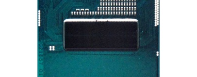
Intel's next-generation processor architecture, Haswell, has been pictured for the first time in a spy shot of an engineering sample.
According to Slovakian technology site OBR-Hardware, the leaked image is of a quality control sample produced at an Intel fabrication facility to prove the next-generation architecture's efficacy ahead of its launch next year.
Built on a 22nm process, Haswell represents the 'tick' portion of Intel's 'tick-tock' development cycle: where the upcoming Ivy Bridge is merely a process size shrink from Sandy Bridge's 32nm to 22nm, Haswell represents a new generation of microarchitecture.
Based on the the existing Core architecture, Haswell promises numerous improvements over its predecessors. The most interesting of these, and sadly invisible in the leaked picture, is HNI: Haswell New Instructions.
Designed to extend the existing instruction set available in Ivy Bridge, HNI includes Advanced Vector Extensions (AVX) 2 with support for SIMD (Single Instruction, Multiple Data) operations on 256-bit integer data types, bit manipulation instructions for improved handling of variable bitstreams, cryptography, compression and large number arithmetic, gather instructions for vectorising codes with non-adjacent data elements, any-to-any permutes with support for DWORD and QWORD granularity permutes across an entire 256-bit register, vector-vector shifts and floating-point multiply accumulate functionality for boosted floating point performance.
In simpler terms: for software designed to take advantage of the new instructions, Haswell promises some significant performance benefits. In particular, better vector handling means vastly improved parallel processing capabilities that could boost overall compute performance significantly for multi-threaded applications.
The image does, however, offer some insight into other aspects of the first Haswell-based processors likely to hit the market: according to OBR-Hardware's analysis of the spy shot, the GPU portion of the die is around twice the size of that included in Sandy Bridge. As a result, we can expect significantly improved graphics performance from the chips.
That observation fits with existing claims - including that from VR-Zone - that Haswell will include multi-standard encode and decode functionality for video resolutions up to QuadHD 4K.
Sadly, with Ivy Bridge not even out of the door yet, Intel is keeping quiet on precise facts and figures for the first Haswell silicon; but it certainly looks like it's going to be a tempting upgrade for performance enthusiasts when it finally hits the market in 2013.
Will you be skipping Ivy Bridge in the hope that Haswell is all that it promises to be, or do you take Intel's proclamations as to the benefits of HNI with a pinch of salt? Share your thoughts over in the forums.


MSI MPG Velox 100R Chassis Review
October 14 2021 | 15:04

Want to comment? Please log in.