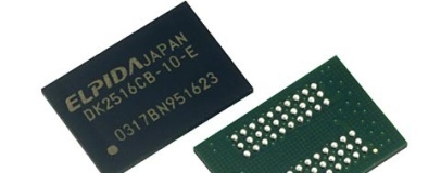
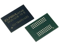
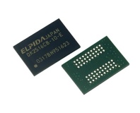
Japanese memory specialist Elpida has announced the development of a resistance memory (ReRAM) prototype, which it claims paves the way for high-speed non-volatile storage that combines the best of DRAM and NAND flash technologies.
Jointly developed with the New Energy and Industrial Technology Development Organisation (NEDO) in Japan, the prototype boasts an overall capacity of 64Mb in a multi-cell array based on a 50nm process size. While that might not sound like much, it's one of the highest capacities yet achieved with ReRAM technology.
As the name suggests, resistance RAM uses a material which changes resistance in response to changes in applied electrical voltage. Because the changes are permanent - at least, until a new voltage is applied to reverse the change - the memory stores its data even when the power is cut, in the same way as the NAND flash cells used in solid-state storage devices.
Unlike NAND flash, however, ReRAM has performance characteristics around the same as dynamic RAM (DRAM), the normal RAM found in a PC which is extremely fast but which wipes its stored data following the loss of power.
According to Elpida's testing, the ReRAM prototype boasts a write speed of 10 nanoseconds and write endurance of one million times, a ten-fold improvement over the best NAND flash currently available.
While not yet ready for commercialisation, Elpida has promised that it will continue developing ReRAM technology in partnership with NEDO, Sharp, the National Institute of Advanced Industrial Science and Technology (AIST,) and the University of Tokyo with a view to producing gigabit-class ReRAM modules in volume using a 30nm process by 2013.
If the company manages to hit its goals, it claims that its ReRAM modules will be a serious competitor to standard NAND flash for smartphone, tablet and ultra-thin laptop storage thanks to both its improved performance and extremely low power draw.
ReRAM isn't the only memory technology which aims to combine the non-volatile nature of flash with the speed of DRAM, however: with IBM continuing its work on magnetoresistive RAM (MRAM) and racetrack memory, HP and Hynix teaming up on memristors for their own ReRAM products and DFG-FET offering yet another route to universal memory, Elpida could have a fight on its hands for a share of that oh-so-lucrative high-performance storage market.
Are you impressed with Elpida's efforts, or saving your applause until the first volume production begins? Share your thoughts over in the forums.


MSI MPG Velox 100R Chassis Review
October 14 2021 | 15:04

Want to comment? Please log in.