GlobalFoundries starts IBM chip production at Fab 8
January 10, 2012 | 10:03
Companies: #globalfoundries #ibm
GlobalFoundries, the chip fabrication specialist born out of AMD, has announced that it has begun production at its latest Fab 8 facility in Saratoga County, New York.
The first components to roll off the company's production, GlobalFoundries has confirmed, will be based on the 32nm silicon-on-insulator technology jointly developed by members of IBM's Process Development Alliance, itself based on research conducted at the University at Albany's College of Nanoscale Science and Engineering.
Designed, GlobalFoundries claims, to vastly improve performance in the areas of multi-core design and graphics, the same SOI design was used in the chips at the heart of Watson, the supercomputer-cum-expert system that shot to fame as a winning contestant on the US gameshow Jeopardy! early last year.
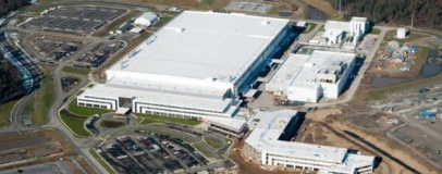
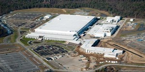
Based in the Luther Forest Technology Campus, Fab 8 is claimed by GlobalFoundries to be the largest leading-edge semiconductor foundry in the world, with 300,000 square feet of clean-room space and a projected output of 60,000 wafers per month once fully ramped. The company has confirmed that production will concentrate on gate-first High-k Metal Gate (HKMG) manufacturing 32nm and 28nm parts, following the company's Fab 1 facility in Dresden hitting volume production on the same process.
Using gate-first, contrasted with gate-last, manufacturing, GlobalFoundries claims, provides a saving of around 10-20 per cent compared to similar HKMG solutions while providing the full benefit of scaling a design down from a 45nm or 40nm process size.
GlobalFoundries won't be the only company making IBM's new chips, however: Big Blue's facility in East Fishkill, some 100 miles south of GlobalFoundries Fab 8, will also be churning out wafers for the company's latest designs.
"Today's announcement is a natural extension of our longstanding partnership with IBM that includes production of 65nm and 45nm chips at our fabs in Singapore and Germany," explained GlobalFoundries chief executive Ajit Manocha. "With the addition of our newest factory in New York, we will now be jointly producing chips with IBM at four fabs on three continents."
The chips, destined for server, storage and supercomputing applications, are also set to feature IBM's embedded DRAM (eDRAM) technology, which boosts on-processor memory performance while reducing component size to a third and standby power to a fifth of traditional SRAM components.
GlobalFoundries commitment to gate-first manufacturing on 32nm and 28nm parts comes despite an announcement from the company in January last year that it would be moving to a gate-last process for 22nm and 20nm parts, joining the majority of the fabrication world in placing the transistors' gates at the end of manufacturing.
Pleased to see GlobalFoundries getting its facilities up and running, or are you waiting to see what the company does at the 20nm process size before getting excited? Share your thoughts over in the forums.
The first components to roll off the company's production, GlobalFoundries has confirmed, will be based on the 32nm silicon-on-insulator technology jointly developed by members of IBM's Process Development Alliance, itself based on research conducted at the University at Albany's College of Nanoscale Science and Engineering.
Designed, GlobalFoundries claims, to vastly improve performance in the areas of multi-core design and graphics, the same SOI design was used in the chips at the heart of Watson, the supercomputer-cum-expert system that shot to fame as a winning contestant on the US gameshow Jeopardy! early last year.
Based in the Luther Forest Technology Campus, Fab 8 is claimed by GlobalFoundries to be the largest leading-edge semiconductor foundry in the world, with 300,000 square feet of clean-room space and a projected output of 60,000 wafers per month once fully ramped. The company has confirmed that production will concentrate on gate-first High-k Metal Gate (HKMG) manufacturing 32nm and 28nm parts, following the company's Fab 1 facility in Dresden hitting volume production on the same process.
Using gate-first, contrasted with gate-last, manufacturing, GlobalFoundries claims, provides a saving of around 10-20 per cent compared to similar HKMG solutions while providing the full benefit of scaling a design down from a 45nm or 40nm process size.
GlobalFoundries won't be the only company making IBM's new chips, however: Big Blue's facility in East Fishkill, some 100 miles south of GlobalFoundries Fab 8, will also be churning out wafers for the company's latest designs.
"Today's announcement is a natural extension of our longstanding partnership with IBM that includes production of 65nm and 45nm chips at our fabs in Singapore and Germany," explained GlobalFoundries chief executive Ajit Manocha. "With the addition of our newest factory in New York, we will now be jointly producing chips with IBM at four fabs on three continents."
The chips, destined for server, storage and supercomputing applications, are also set to feature IBM's embedded DRAM (eDRAM) technology, which boosts on-processor memory performance while reducing component size to a third and standby power to a fifth of traditional SRAM components.
GlobalFoundries commitment to gate-first manufacturing on 32nm and 28nm parts comes despite an announcement from the company in January last year that it would be moving to a gate-last process for 22nm and 20nm parts, joining the majority of the fabrication world in placing the transistors' gates at the end of manufacturing.
Pleased to see GlobalFoundries getting its facilities up and running, or are you waiting to see what the company does at the 20nm process size before getting excited? Share your thoughts over in the forums.


MSI MPG Velox 100R Chassis Review
October 14 2021 | 15:04

Want to comment? Please log in.