
COMPUTEX 2009: We dropped into ECS HQ in Taipei and caught a glimpse of its upcoming live demo for next week's Computex.
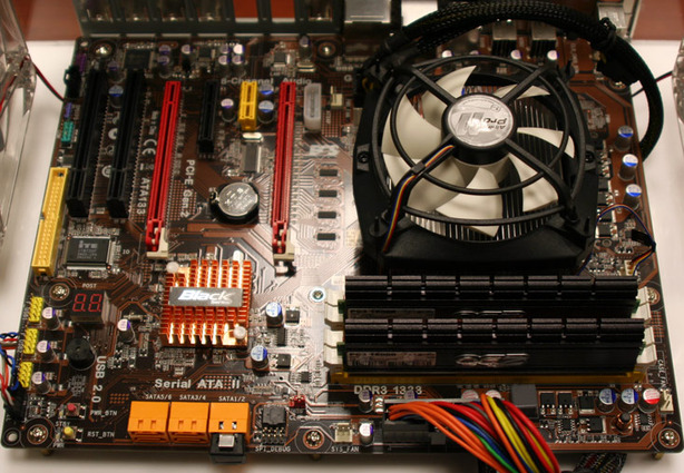
The Lynnfield CPU socket itself is, well, strange, with the abnormally large retention clip. The actual socket size and CPU are similar to LGA775, however the pin pitch is largely reduced to pack more in to make up the extra few hundred to 1156.
ECS P55H-A motherboard sports a few new features like an automatic power phase indicator to show how many power phases are being used by the CPU, as well as a copper P55 heatsink as well.
For the rest, it's pretty standard affair, with dual x8 (x16 physical) lanes from the CPU, dual channel DDR3 1,333MHz, PCI-Express x1, x4 and two PCI slots. There are no extra SATA ports other than the standard six and ECS does frankly quite little in the way of unique features. Still.
Discuss in the forums.
RELATED ARTICLES


MSI MPG Velox 100R Chassis Review
October 14 2021 | 15:04

Want to comment? Please log in.