
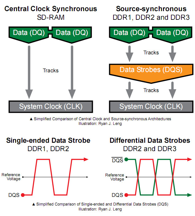
Source-Synchronous Architecture
One of the most significant changes introduced in DDR1 was the step away from relying on a central clock scheme used in SDR, to introducing a Source-Synchronous or Strobing design.The benefit of which was a requirement for higher performance. The introduction of a single-ended Data Strobe (DQS) architecture creates an additional tracking layer between the Data and the centralised System Clock (CLK).
DDR1’s “Single-ended” Data Strobe refers to the characteristic of having only a single rising and falling signal wave. This single-ended Data Strobe is tracked by the Data (DQ) for more effective signalling – it has greater fundamental strength in tolerating Process-Voltage-Temperature (PVT) variation and issues caused by crosstalks, echoes and signal reflection, which tend to distort the waveform or induce timing inaccuracy.
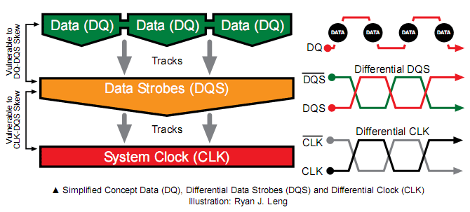
The objective to introduce an additional timing layer known as the Data Strobe was to help the Data track the clock more effectively at higher speed grades; however this also creates extra complexity.
Despite the Data Strobe easing the timing inaccuracy between the Data and the System Clock at higher frequency, the Data Strobe itself can fall out of alignment or skew with the System Clock. As a result, an additional “De-skewing” or synchronization logic has to be built between these two to ensure proper operation.
What is this thing called the Data Strobe or DQS?
The Data Strobe is a tracking guide for data against the System Clock. It is an oscillating electrical signal that defines where the data must be at and how long it should be there.As the name Synchronous Dynamic (SD) RAM implies, modern computer memory relies on everything lining up to a centralised clock for reliable signalling. It was first introduced in DDR1 with a single-ended design. At higher DDR2 speeds, a differential strobing design was required.
Aaron Boehm, Application Engineer at Micron Technology, explains that the problem “is that the clock can vary quite a bit, so the DQS is used to line all your data up to the clock. Internal to the DRAM, the strobe tracks the clock. So when the DRAM outputs the data, the data is aligned to the strobe which tracks the clock. When the memory controller writes to the DRAM, that data centralised to the strobe. The data strobe (DQS) allows both the controller as well as the DRAM to look at that and lock in the data.”
RELATED ARTICLES


MSI MPG Velox 100R Chassis Review
October 14 2021 | 15:04

Want to comment? Please log in.