Size Matters: Shrinking to 16nm
One of the key enablers of the performance and efficiency gains Nvidia has made with Pascal is the shift to a smaller manufacturing process, specifically TSMC's 16nm FinFET node. While AMD was the first to shift to 28nm way back in 2011, Nvidia has beaten the red team to the punch here, with Polaris (AMD's new architecture using a GlobalFoundries 14nm FinFET process) not due until the end of this month.Continually shrinking transistors is no easy task, as you start to encounter unhelpful elements of the laws of physics like quantum tunnelling and various short-channel effects. Indeed, the 20nm node was abandoned altogether by TSMC, and 16nm was also beset by delays.
Click to enlarge
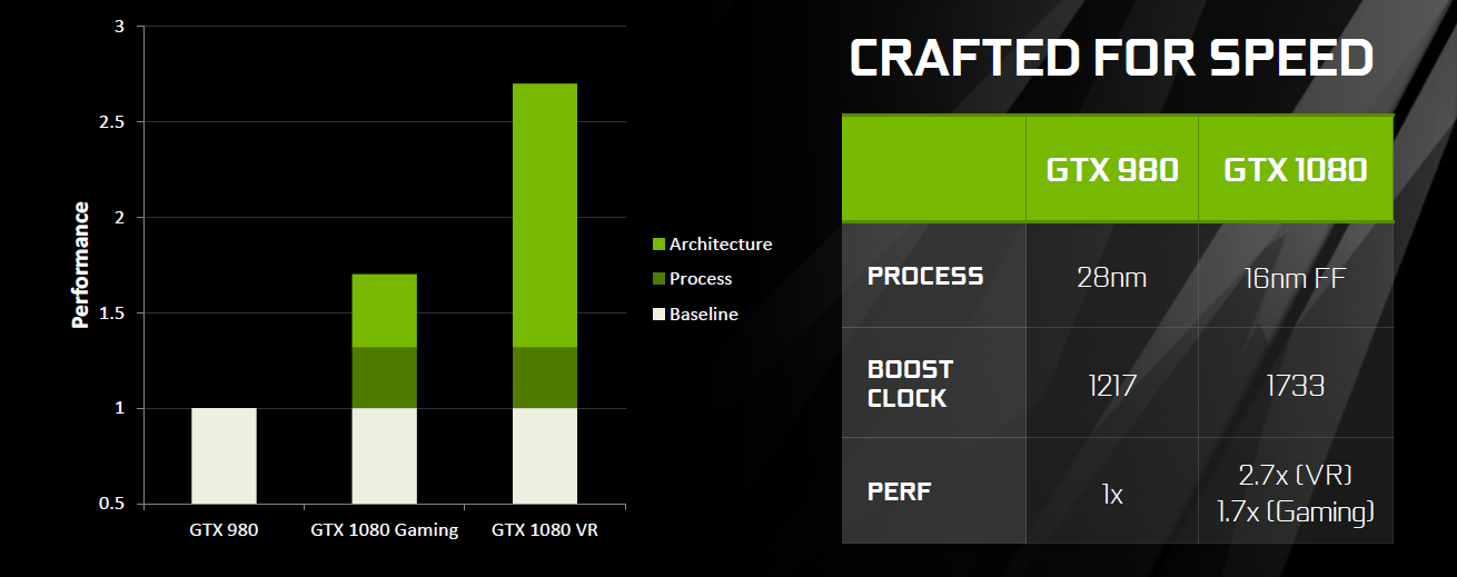
Still, the issues have been overcome enough for mass production to begin. Using smaller transistors allows Nvidia to cram more into a given area, and get more GPU dies from a single wafer, helping to offset the initial research and development costs in the long term. More importantly for consumers, the transistors require less current to operate, thus reducing power consumption and increasing the clock speed headroom.
The effects of the shrink are clear. The GP104 GPU used in the GTX 1080 crams 7.2 billion transistors into a die size of just 314mm2. To put that in perspective, the 28nm GM204 used by the GTX 980 had only 5.2 billion transistors but was 398mm2, while the 8 billion transistor GM200 (GTX 980 Ti and GTX Titan X) measured 601mm2. Clearly, plenty of space is being saved.


MSI MPG Velox 100R Chassis Review
October 14 2021 | 15:04

Want to comment? Please log in.