Nvidia GeForce GTX 970 Review Roundup: feat. ASUS, EVGA and MSI
September 19, 2014 | 16:56
Nvidia GeForce GTX 970 Review Roundup: feat. ASUS, EVGA and MSI
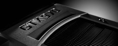
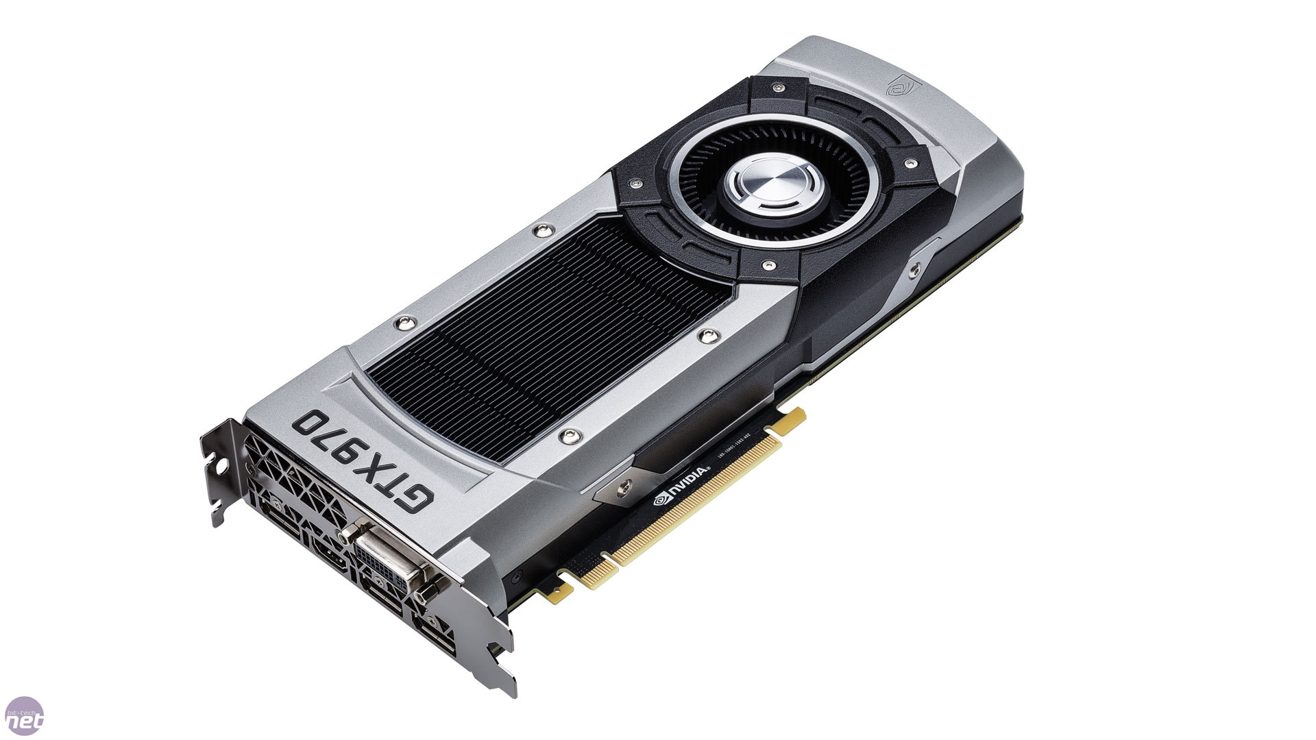
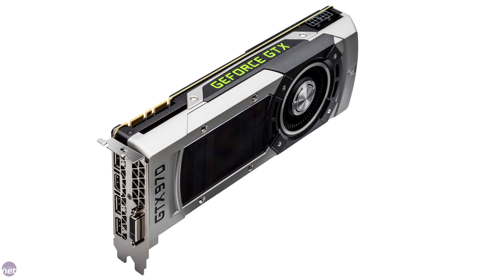
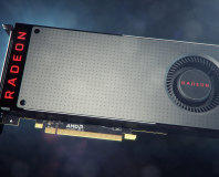
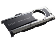
If you've already worked your way though our GTX 980 review, then you'll know that unlike that card, Nvidia is not producing a reference model of the GTX 970, the second enthusiast-grade Maxwell part that replaces the GTX 770 in the product stack. The images on this page do not reflect a ready to buy product. Instead, Nvidia's AICs will be able to purchase the GPU and memory chips, but after that it's up to them, and this will undoubtedly lead to a high degree of variability when it comes to PCB and cooler design as well as factory overclocks. Pricing is set to start at £259 inc VAT here, which is a significantly lower price than the £429 of the GTX 980 considering that the specs aren't that far apart.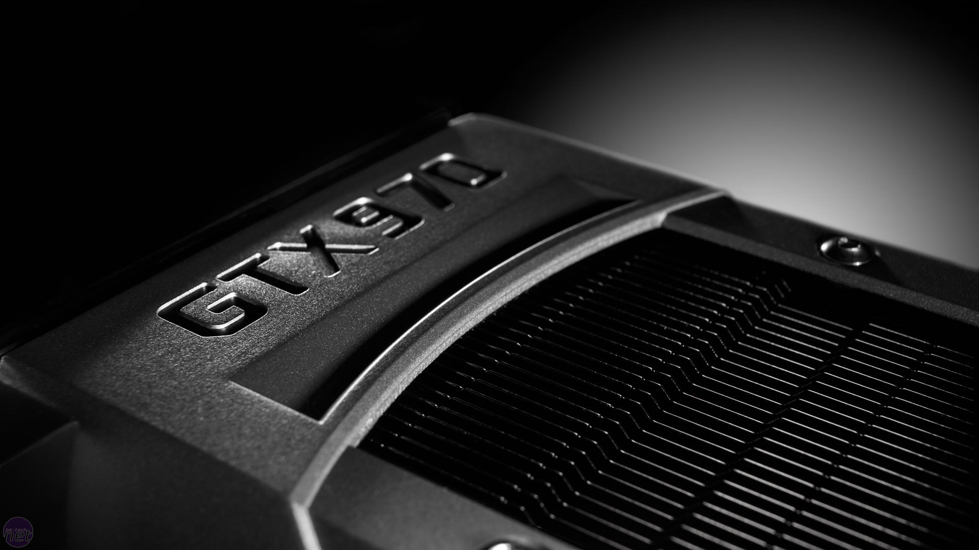
Click to enlarge
As such, we're approaching this review slightly differently to usual, and we'll be testing three different GTX 970 cards from three of Nvidia's key partners: ASUS, EVGA and MSI. All three ship with custom coolers and factory overclocks, so it will be interesting to see how well they cool themselves and how much further they can be replaced.
If you haven't read the GTX 980 review, then that's where you'll need to head for all the technical specifics on the new GM204 GPU and its new display and graphics processing capabilities.
In summary, however, GM204 is Nvidia's enthusiast level Maxwell GPU, fully enabled in the new flagship GTX 980, and slightly cut down in this here GTX 970, as the specs table illustrates.
| Nvidia GeForce GTX 980 4GB | Nvidia GeForce GTX 970 4GB | Nvidia GeForce GTX 780 Ti 3GB | Nvidia GeForce GTX 780 3GB | Nvidia GeForce GTX 680 2GB | |
| GPU | |||||
| Architecture | Maxwell | Maxwell | Kepler | Kepler | Kepler |
| Codename | GM204 | GM204 | GK110 | GK110 | GK104 |
| Base Clock | 1,126MHz | 1,050MHz | 876MHz | 836MHz | 1,006MHz |
| Boost Clock | 1,216MHz | 1,178MHz | 928MHz | 900MHz | 1,058MHz |
| Stream Processors | 2,048 | 1,664 | 2,880 | 2,304 | 1,536 |
| Layout | 4 GPCs, 16 SMMs | 4 GPCs, 13 SMMs | 5 GPCs, 15 SMXs | 4 GPCs, 12 SMXs | 4 GPCs, 8 SMXs |
| Rasterisers | 4 | 4 | 5 | 4 | 4 |
| Tesselation Units | 16 | 13 | 15 | 12 | 8 |
| Texture Units | 128 | 104 | 240 | 194 | 128 |
| ROPs | 64 | 64 | 48 | 48 | 32 |
| Transistors | 5.2 billion | 5.2 billion | 7.1 billion | 7.1 billion | 3.54 billion |
| Die Size | 398mm2 | 398mm2 | 533mm2 | 551mm2 | 294mm2 |
| Process | 28nm | 28nm | 28nm | 28nm | 28nm |
| Memory | |||||
| Amount | 4GB GDDR5 | 4GB GDDR5 | 3GB GDDR5 | 3GB GDDR5 | 2GB GDDR5 |
| Frequency | 1.75GHz (7GHz Effective) | 1.75GHz (7GHz Effective) | 1.75GHz (7GHz Effective) | 1.5GHz (6GHz Effective) | 1.5GHz (6GHz Effective) |
| Interface | 256-bit | 256-bit | 384-bit | 384-bit | 256-bit |
| Bandwidth | 224GB/sec | 224GB/sec | 336GB/sec | 288GB/sec | 192GB/sec |
| Card Specifications | |||||
| Power Connectors | 2 x 6-pin PCI-E | 2 x 6-pin PCI-E | 1 x 6-pin, 1 x 8-pin PCI-E | 1 x 6-pin, 1 x 8-pin PCI-E | 2 x 6-pin PCI-E |
| Stock Card Length | 267mm | 267mm | 267mm | 267mm | 252mm |
| TDP | 165W | 145W | 250W | 250W | 195W |
In the GTX 970, three of the 16 SMMs are disabled, leaving the card with a total of 1,664 CUDA cores, 13 geometry/tesselation units and 104 texture units. As is common practice, Nvidia does not disclose which SMMs are disabled. It actually varies from GPU to GPU, though not in a way that affects performance, and this allows Nvidia to get the best yield from chips that don't make it through the manufacturing process with all the SMMs intact.
Clock speeds have been lowered slightly too, although they're still relatively high. The GTX 970 has a base clock of 1,050MHz and a rated boost clock of 1,178MHz, which represents the average frequency the cards will boost to in normal gaming workloads – exact frequencies will vary. However, it should also be pointed out that these reference clock speeds are really only that – for reference only. Most partners will opt for a factory overclock of some sort on each of the SKUs they release.
Other than this, the specifications are largely the same. The 4GB GDDR5 frame buffer is left at full capacity. The GPU communicates with this via a 256-bit bus (four 64-bit memory controllers) at an effective data rate of 7GHz for a total memory bandwidth of 224GB/sec. This is on the low side for a high-end GPU these days, but as discussed in the GTX 980 review, Nvidia reduces the need for memory bandwidth by introducing a large, shared L2 cache of 2MB (higher than even GTX Titan) and by a technique referred to as third generation delta colour compression, which compresses frame data in a lossless fashion on-the-fly, saving on average 25 percent of memory bandwidth. Rounding out the GTX 970 GPU at the back-end is the full complement of 64 ROPs.
Click to enlarge
The GTX 970 supports all of the major display technologies introduced with the GTX 980, including Voxel Global Illumination, Dynamic Super Resolution and Multi-Frame Sampled AA. Again, for a full rundown of these you'll want to head here.
Efficiency is the name of the game with Maxwell, and the already low TDP of the GTX 980 has been reduced even further for the GTX 970, from 165W to 145W, which is 85W lower than the card it replaces, the GTX 770. Power is supplied (at least in the reference specifications) through two 6-pin PCI-E power connectors, via a 4+1 phase power delivery system.
Finally, the reference display connections are the same as those of the GTX 980: a single dual-link DVI-I, three DisplayPorts (version 1.2) and a HDMI port, which is version 2.0 and thus capable of powering 4K displays at 60Hz all by itself. Of course, actual display configurations are likely to vary from partner to partner, but what doesn't vary is that the GTX 970 can support up to four displays at once. G-Sync is of course also support via DisplayPort.


MSI MPG Velox 100R Chassis Review
October 14 2021 | 15:04

Want to comment? Please log in.