
AMD Radeon HD 7970 3GB Review
Manufacturer: AMDUK Price (as reviewed): Released 9 January 2012, approx. £440 (inc VAT)
US Price (as reviewed): Released 9 January 2012, $549 (ex tax)
It’s been a quiet year for graphics. With both AMD and Nvidia playing their current generation’s hand by March 2011 with the arrival of the GeForce GTX 590 3GB and the Radeon HD 6990 4GB, the rest of the year has only seen minor or limited-run releases such as the GeForce GTX 560 Ti 448 1.3GB or the Radeon HD 6790 1GB.
However, with Intel’s Ivy Bridge processor rumbling closer, the next round of upgrades beckons, and it’s AMD that’s first out of the traps with the Radeon HD 7970 3GB, the world’s first consumer 28nm GPU. This will be the first of a whole new family of 28nm HD 7000-series GPUs, the rest of which will be released gradually over the first six months of 2012. For now though, the HD 7970 3GB will co-exist with the existing HD 6000-series GPUs, and its £440 price puts it well into the premium graphics bracket.


Ohhhhh, Shiny....
Out with the old, in with the new
Codenamed Tahiti XT, AMD has made some radical changes for its first 28nm GPU. The entire stream processor layout has been altered, with the 24 SIMD Engines of Caymen XT replaced by 32 individual compute units (CUs), which AMD has chosen to dub Graphics Core Nexts (GCNs). Poor English aside, each CU (no, we’re not going to call them GCNs) contains four SIMD Engines, with each of these equipped with 16 stream processors and its own vector units and 64KB vector register. This means each CU therefore includes 64 stream processors and the GPU as a whole wields 2,048 stream processors; 512 more than the previous top-end Caymen XT.Out of the box the GPU runs at 925MHz - a 5 per cent increase over the HD 6970 2GB’s 880MHz frequency. Each CU is also equipped with four texture units (the same as for each SIMD Engine in Caymen XT), resulting in a total of 128 texture units for the whole GPU.
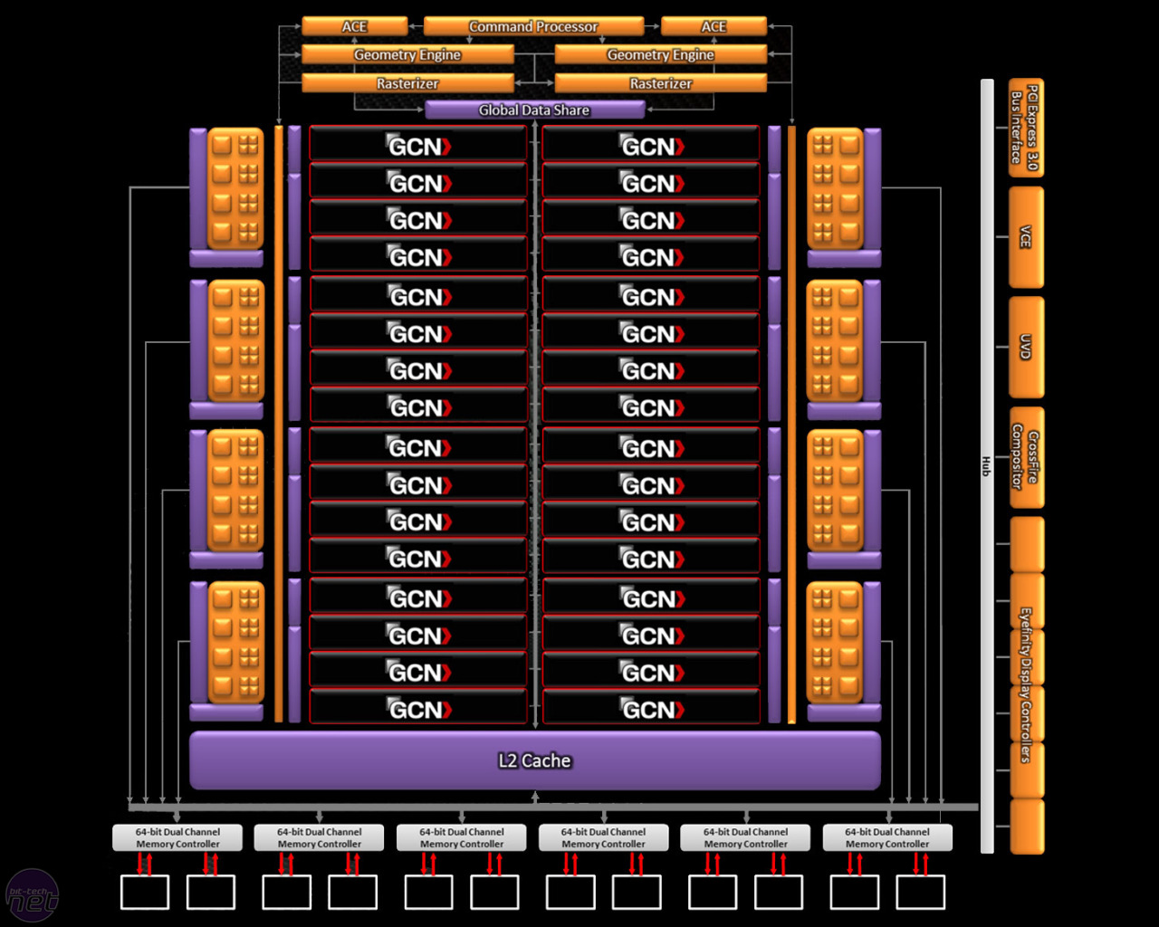
The Tahiti XT architecture is a big change for AMD
The new CU layout also sees the abandonment of the VLIW (Very Long Instruction Word) design philosophy that has typified AMD GPUs as far back as the Radeon HD 2900 XT. This is a significant change for AMD, and brings it into line with Nvidia’s modular Fermi-based GPUs. AMD claims the move away from VLIW, along with the new CU layout, significantly simplifies the GPU’s render process, making the GPU’s performance more predictable and in need of less optimisation.
As we’ve already said, AMD has once again used a dual front-end engine design for Tahiti XT, although it’s notably different from that of its predecessor. Each front end unit’s geometry assembler, vertex assembler and ninth generation tessellator have been merged into a geometry engine, with the rasteriser in a separate unit. AMD claims this new layout has significantly improved the GPU’s tessellation performance, with up to four times the throughput of the HD 6900 design. Also new to the pair of front end engines is an asynchronous compute engine (ACE) each, further underlining AMD’s focus on GPGPU performance by allowing compute and graphics operations to enter the GPU simultaneously.
The GPU’s memory has also been given a boost. Six 64-bit dual channel memory controllers each connect to two 256MB GDDR5 memory modules, making for a staggering 3GB of video memory in total, which is connected via a fat 384-bit bus. Combined with a memory frequency of 1,375MHz (5.5GHz effective), the HD 7970 3GB boasts a mighty 264GB/sec of memory bandwidth, making it well suited to ultra-high resolutions such as those of Eyefinity setups.
Rounding out the GPU’s vital statistics are eight render back-end units, each with four ROPs for a combined total of 32 ROPs, which has been the standard number for AMD’s high end GPUs for the last few generations. All in all AMD has somehow managed to cram 4.3 billion transistors into the 365mm² GPU die; an increase of 65 per cent compared with the previous high-end Cayman XT GPU, and in a 6 per cent smaller die.
RELATED ARTICLES


MSI MPG Velox 100R Chassis Review
October 14 2021 | 15:04

Want to comment? Please log in.