Is Half a Fermi a Semi?
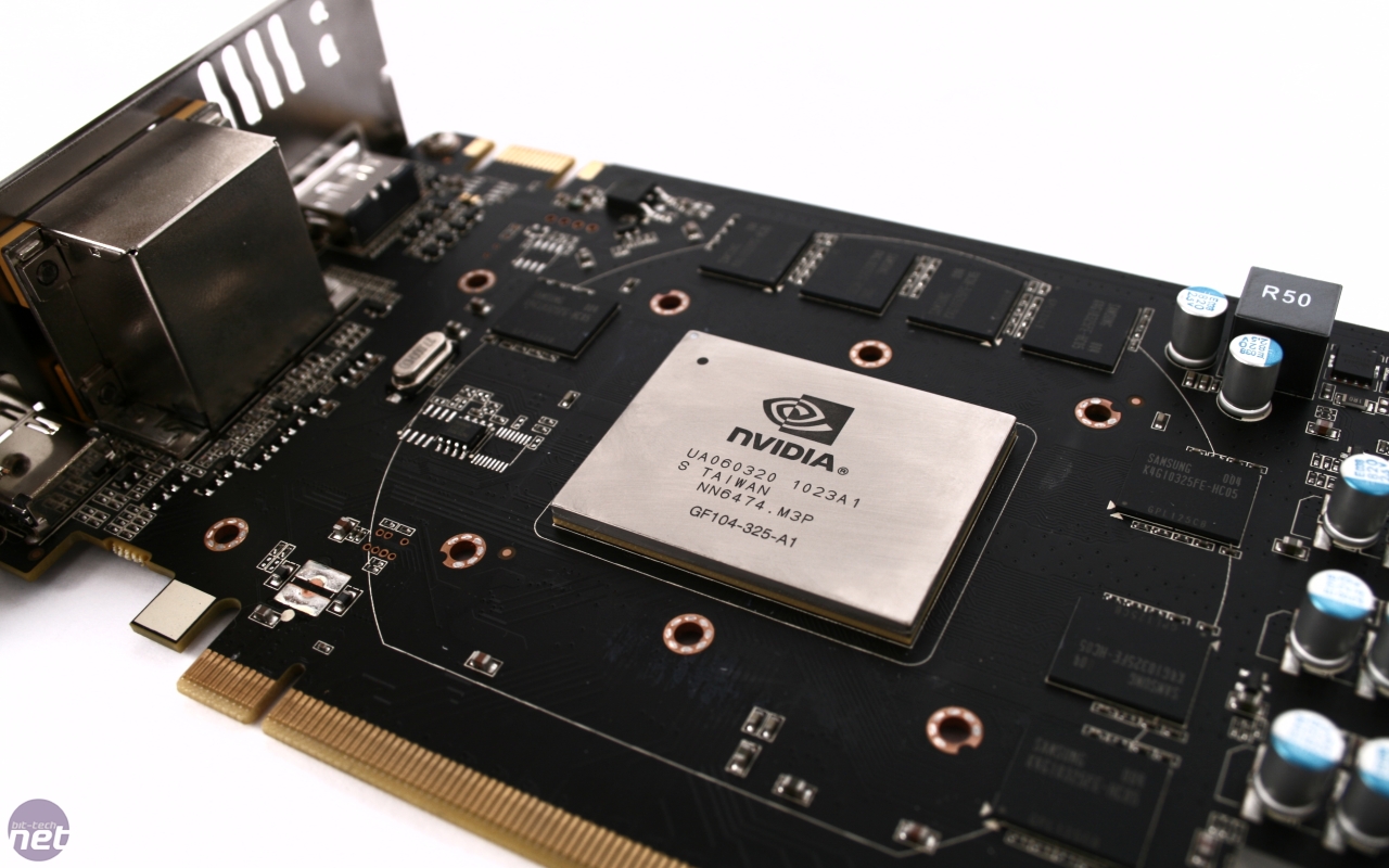
Nvidia’s claims that its Fermi architecture is modular certainly seem true – the new GTX 460 (codenamed GF104) has two GPCs to the four of the GF100-based GTX 480 and GTX 470. However, the GTX 460 isn’t exactly half a GTX 480 – Nvidia has enhanced the SMs of the original design so that the GTX 460 has 70 per cent of the stream processors that a GTX 480 has rather than 50 per cent. The frequencies of the GTX 460 are between those of the GTX 480 and the GTX 470 too, meaning that on paper the GTX 460 looks rather promising.Nvidia says that it ‘could have cut the GeForce GTX 480 GPU in half [when designing the GTX 460], however, we wanted to tailor the chip to nail the gamers sweet spot segment.’ We hope that won’t be quite as painful as it sounds. Claiming the GTX 460 to ‘deliver the perfect blend of performance, price and power [consumption]’ does sound as if Nvidia has learnt from the mistakes of the past – the GTX 480 was hugely overpriced at launch, and the same could be said of the GeForce GTX 280 and GTX 260 when they launched.
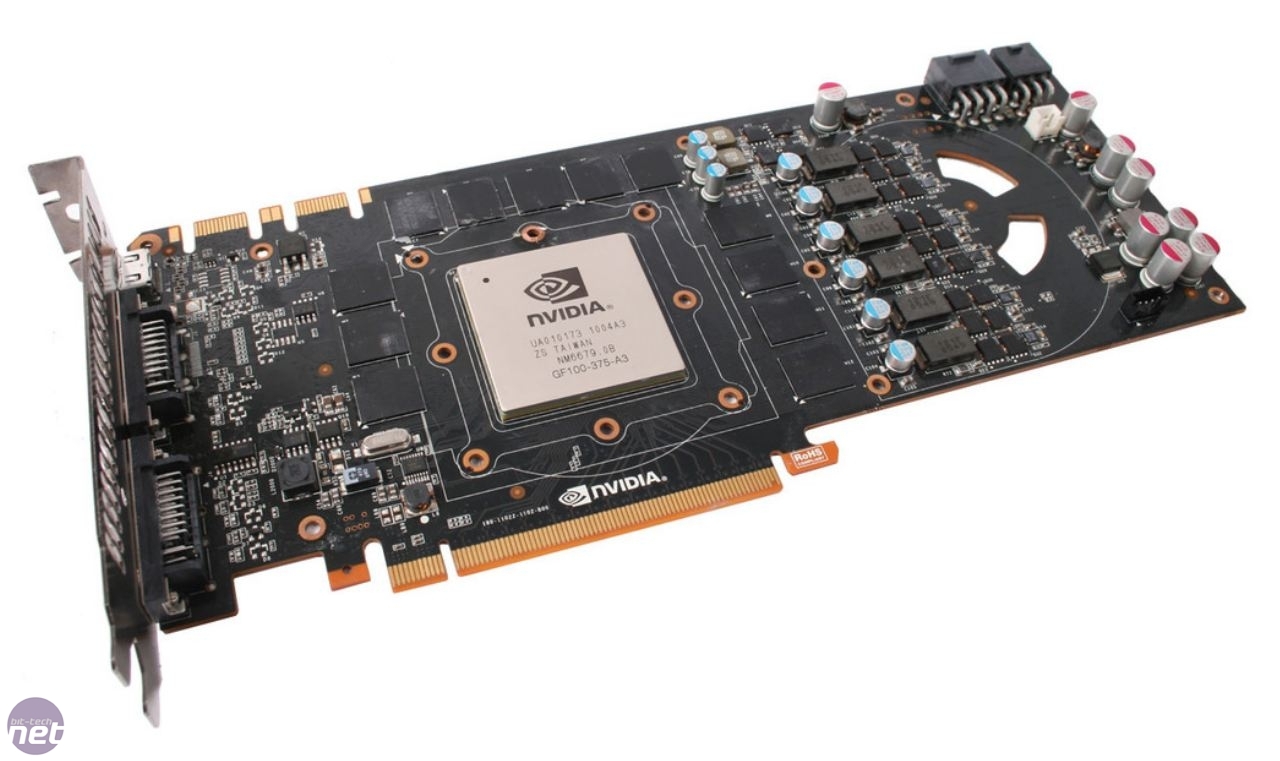
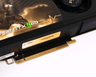
The new GTX 460 is more oblong than its GTX 480 sibling (left) as it only has two GPCs, even if these contain more resources each. Click to enlarge
The reality of these claims is that each SM of the GTX 460 has 48 stream processors (which we still refuse to call CUDA cores as Nvidia would like) rather than the 32 stream processors per SM of the original GF100 design. This has necessitated an increase in the number of texture units per SM too, from the four of the original design to eight. The SMs of the GTX 460 are arranged into a group of four in one GPC and a group of three in the other.
Two Versions of the GTX 460
There are two versions of the GTX 460 to look out for, with the differentiator being the amount of memory on the card. However, there are more differences than merely whether the card has 768MB of memory or 1GB. As the difference is in the number of memory chips (rather than the density), there are fewer memory controller units enabled on the lesser 768MB version, fewer ROPs (24 rather than 32) and less Level 2 cache (384KB, not 512KB). Essentially, the memory sub-system has been slightly cut back, either because of defects in the manufacturing process or just to hit a lower price (or both).It’s only the memory subsystem that differs between the two GPUs though, with the specs elsewhere identical. Both cards therefore have 336 stream processors running at 1,350MHz, while the rest of the GPU is clocked at 675MHz. Whether a (standard) GTX 460 has 1GB of GDDR5 memory or just 768MB, it runs at 900MHz (3.6GHz effective) too. Standard GTX 460 768MB cards are due to cost £180, while a standard 1GB 1GB card will cost £200 – this puts the two cards up against ATI’s Radeon HD 5830, though we also tested the £140 HD 5770 and £230 HD 5850.
Possibly the most interesting point to raise from the specs below is that the GTX 460 looks to be faster than the GTX 465, despite the latter’s superior name. The 352 stream processors of the GTX 465 operate at 1,215MHz while the 336 stream processors of the GTX 460 run at 1,350, giving the GTX 465 a maximum ‘stream processor operations per second’ of 427,680 rather than 453,600. We know this number only gives a rough estimation of relative performance, but we’ll be keen to see if Nvidia has dropped another naming clanger.
| Mid-range DirectX 11 Graphics Cards | |||||||
| ATI Radeon HD 5850 | ATI Radeon HD 5830 | ATI Radeon HD 5770 | Nvidia GeForce GTX 470 | Nvidia GeForce GTX 465 | Nvidia GeForce GTX 460 1GB | Nvidia GeForce GTX 460 768MB | |
| Price | £240 | £165-£190 | £130 | £260 | £200 | Around £200 | Around £180 |
| Manufacturer | ATI (AMD) | ATI (AMD) | ATI (AMD) | Nvidia | Nvidia | Nvidia | Nvidia |
| GPU | |||||||
| Codename | Cypress Pro | Cypress LE | Juniper XT | GF100 | GF102 | GF104 | GF104 |
| GPU Frequency | 725MHz | 800MHz | 607MHz | 607MHz | 675MHz | 675MHz | |
| Stream Processors | 1,440 | 1,120 | 800 | 448 | 352 | 336 | 336 |
| Stream Processor Frequency | 725MHz | 800MHz | 850MHz | 1,215MHz | 1,215MHz | 1,350MHz | 1,350MHz |
| Texture Units | 72 | 56 | 40 | 56 | 44 | 56 | 56 |
| ROPs | 32 | 16 | 16 | 40 | 32 | 32 | 24 |
| Transistors | 2.15bn | 2.15bn | 1.04bn | 3bn | 3bn | 1.95bn | 1.95bn |
| Manufacturering Process | 40nm | 40nm | 40nm | 40nm | 40nm | 40nm | 40nm |
| MEMORY | |||||||
| Memory | 1GB GDDR5 | 1GB GDDR5 | 1GB GDDR5 | 1,280MB GDDR5 | 1GB GDDR5 | 1GB GDDR5 | 768MB GDDR5 |
| Frequency | 1GHz (4GHZ effective) | 1GHz (4GHZ effective) | 1.2GHz (4.8GHz effective) | 837MHz (3.3GHz effective) | 800MHz (3.2GHz) | 900MHz (3.6GHz effective) | 900MHz (3.6GHz effective) |
| Memory Interface | 256-bit | 256-bit | 128-bit | 320-bit | 256-bit | 256-bit | 192-bit |
| Bandwidth | 128GB/sec | 128GB/sec | 77GB/sec | 134MB/sec | 102GB/sec | 115GB/sec | 86GB/sec |
| CARD | |||||||
| Power Connections | 2 x 6-pin PCI-E | 2 x 6-pin PCI-E | 1 x 6-pin PCI-E | 2 x 6-pin PCI-E | 2 x 6-pin PCI-E | 2 x 6-pin PCI-E | 2 x 6-pin PCI-E |
| Maximum Power Consumption | 151W | Varies | 108W | 215W | Varies | 160W | 150W |
| Recommended Power Supply* | 500W | 500W | 450W | 550W | 550W | 450W | 450W |
| Size | 9in long, dual slot | Varies, dual slot | 8.25in long, dual slot | 9.5in long, dual slot | 9.5in long, dual slot | 8.25in long, dual slot | 8.25in long, dual slot |
| *Manufacturer recommendation only, this may not represent bit-tech's own recommendations | |||||||
RELATED ARTICLES


MSI MPG Velox 100R Chassis Review
October 14 2021 | 15:04

Want to comment? Please log in.