
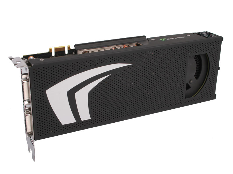
Nvidia GeForce GTX 295 1,792MB & Quad SLI
Manufacturer: NvidiaUK Pricing: £400 (inc. VAT) - estimated
US Pricing: $499 MSRP
Core Clock: 576MHz
Shader Clock: 1,242MHz
Memory Clock: 1,998MHz
Memory: 1,792MB GDDR3
Just a week before Christmas, Nvidia allowed us to disclose some early performance numbers for its next flagship part, the GeForce GTX 295. Because the card was still a few weeks away from release, there were some restrictions which we detailed in the first page of that performance preview.
Today, being the first day of CES proper, is D-day for the GeForce GTX 295 and we're finally able to talk about the card without any restrictions in place. Over the coming pages, we will be discussing the card in a lot more detail than we did before and we'll be disclosing performance – in both single and dual-card Quad SLI configurations – as well as looking at power consumption and heat. I'm sure the question that is on most people's mind is whether or not the GeForce GTX 295 does enough to topple AMD's ATI Radeon HD 4870 X2? I guess we should get on and find out!
Click to enlarge
All about the 55nm GT200b
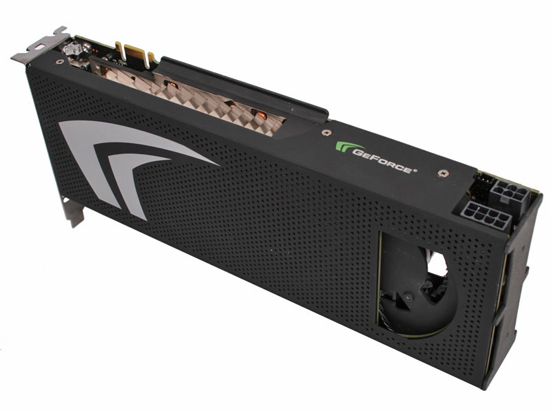
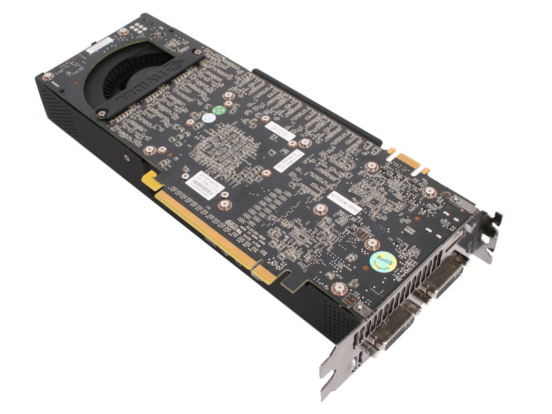
If you've already read our initial preview, you'll know that the GeForce GTX 295 combines a pair of 55nm GT200b chips on a single graphics card. It uses a similar design to the GeForce 9800 GX2, as the GPUs are on separate PCBs that face one another with a cooler sandwiched between them. From everything we've heard from various sources – both official and unofficial – GT200b is simply a die shrink of the original GT200 A2 silicon with a few tweaks. It's GT200's B3 stepping, essentially – just manufactured on one of TSMC's 55nm nodes.There are some improvements, but nobody would go into detail on exactly what those improvements were – Nvidia says that there are some timing changes that are designed to improve performance per watt so that the GeForce GTX 295 remains feasible. Of course, a maximum board power of 289W is pretty high, but it's not alarmingly high when you consider that the ATI Radeon HD 4870 X2's maximum board power is quoted at 286W.
In addition to making the GTX 295 a feasible product – and one that wouldn't have been viable with a pair of 65nm GT200 chips – the tweaks made to the B3 stepping also means higher clocks can be achieved with single GPU graphics cards – like the upcoming GeForce GTX 285 – as well.
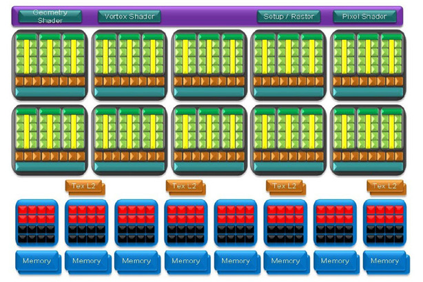
Nvidia's GT200 GPU flow diagram
There are the full 240 stream processors enabled on each of the GPUs, meaning 480 in total. These are clocked at 1,242MHz – the same speed as they are clocked on the GeForce GTX 260 (both revisions). As the texture units are associated with each stream processing cluster, there is a full allocation of 80 per GPU, eight per stream processing cluster and 160 in total. When combined with a 576MHz ‘core’ speed, this results in an impressive texture throughput of 92.2 GigaTexels per second.
Each chip backs out onto 28 ROPs (or render backends), making a total of 56 in total and, like previous GPUs derived from Nvidia’s G80 graphics processor, they run at the same speed as the texture units and setup engine. This means there is a 448-bit memory interface per GPU and Nvidia has kitted each GPU out with 896MB of memory (1,792MB in total) clocked at 1,998MHz effective.
What we’re looking at, then, is essentially a pair of GeForce GTX 260-216 graphics cards in SLI, but with 240 stream processors per GPU instead of 216. This was something that confused us a little because, when we reviewed the GeForce GTX 260-216, we came to the conclusion that it was running out of memory bandwidth – there were many scenarios where the GeForce GTX 260-216 wasn’t discernibly faster than the original GeForce GTX 260.
Click to enlarge
Nvidia said that it needed to leave headroom for partners to create their own versions, but an additional 200MHz or so on the memory would have helped prevent the GeForce GTX 295 from becoming bandwidth starved at higher resolutions – in both single and dual-card setups. We saw evidence of this problem cropping up in our preview, and we've seen more in the fairly extensive testing we've done since then.
One thing that Nvidia doesn't want to talk about at the moment, despite our repeated probing, is the GT200b's die size – all we know is that it's obviously smaller than the GT200 A2 silicon we saw in June. Doing a quick calculation based on the GT200's 576mm² die size brings us to an area of 412mm², but that is only if the shrink was 100 percent linear. We know that Nvidia has made some tweaks and optimisations and even though the transistor count remains around the 1.4 billion mark, the shrink may not be linear, but 412mm² represents a fairly well educated estimation.
RELATED ARTICLES


MSI MPG Velox 100R Chassis Review
October 14 2021 | 15:04

Want to comment? Please log in.