
RV770 Graphics Architecture
During the many discussions I had with several members of the team involved in RV770’s development, it quickly became apparent that the focus of the architecture was on efficiency in just about every way imaginable. AMD said that it worked to optimise the original R600 design by taking the elements of the architecture and improving upon them to create a more balanced—and efficient—graphics processing unit.At many points during my conversations, AMD said that it was no longer making big GPUs, but I beg to differ with those statements because RV770 isn’t what I'd call a ‘small’ GPU – it has just shy of one billion transistors (956m to be exact) packed into the 260mm² die fabricated on one of TSMC’s 55nm nodes. What it is though is an efficient use of die space and when the company’s execs were discussing this fact, it turned out to be a chance for AMD to poke fun at Nvidia’s GT200 chip and lately, at least, the two seem quite eager to poke fun at one another.
For the sake of completeness, GT200 packs 1.4 billion transistors into a die with a surface area of somewhere between 500mm² and 600mm² using TSMC’s 65nm process technology. We’re led to believe that the actual size is much closer to the latter than the former, although Nvidia won’t be any more specific than the incredibly vague range it disclosed to us during our roundtable discussions in May.
Just looking at those numbers highlights the levels of efficiency AMD has achieved with RV770 on the manufacturing front. Of course, it’d be wrong not to mention the fact that AMD has a process technology advantage in its hand, but it’s only an optical shrink and not a complete reworking of the tools. What this means is that the benefits of the smaller process technology aren’t quite as significant as they are when you shrink the tools as well.
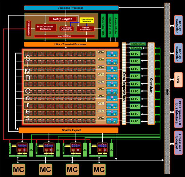
AMD's ATI RV770 GPU block diagram
The architecture itself is very similar to AMD’s previous unified shader architecture, so if you’re familiar with the R600 and RV670 designs, you should find it easy to understand what’s going on inside RV770. However, that’s not to say RV770 is exactly the same as what’s come before and there have been a number of quite significant refinements.
The design is still very much based on the VLIW (very long instruction word) idea introduced with the Radeon HD 2900 XT and each shader processor is made up of five stream processors each with different levels of functionality. When the ill-fated 2900 XT launched, we were more than a little sceptical about some of the architectural decisions made, but that was more down to problems outside of the VLIW design that really hampered the card’s performance – here, I’m referring to things like the broken anti-aliasing resolve units as one of the major design killers.
Both the Radeon HD 4850 and Radeon HD 4870 feature a ‘full-fat’ RV770 chip, meaning they both feature 160 five-way VLIW superscalar shader processors or 800 stream processors in total, 40 texture units and 16 ROPs that back out onto a 256-bit memory interface. The difference between the two, then, lies in clock speed and memory type – the Radeon HD 4850 is conservatively clocked and uses 512MB of GDDR3 memory, while the Radeon HD 4870 comes with a more aggressive core speed and features 512MB of super-high-speed GDDR5.
Tessellation now available in DX10
DirectX 10.1 support is present as expected and the drum is being banged even harder than before. There are now four announced DirectX 10.1 games--Assassin's Creed, Battleforge, Storm Rise and Cloud 9--but I've only heard of two of them and one of those had DirectX 10.1 support removed after the first patch.I asked bit-tech's resident games expert and he said he's only heard of two of them as well - what this means is that we'll have to wait and find out if the games are worth playing when they're released. Saying a title that nobody knows about (nay, cares about) supports a feature one company is trying to push is a much of a muchness in my opinion.
The tessellation unit is also present and it's similar in capabilities to the one featured in both R600 and RV670, but this implementation has been made more accessible to developers. With the previous generation hardware, the tessellator was not available to developers in DirectX 10 and could only be used with DirectX 9.0 – it’s now accessible through both DirectX 10 and 10.1.
Additionally, during a discussion I had with one of the architects, I learned that the tessellation unit inside RV770 can now export data to the geometry shader. This is great news because the two can work together hand-in-hand to deliver some awesome procedurally generated triangles and detail. When asked, AMD said that it might be possible to achieve the same effects without a tessellation unit using only the geometry shader, but the tessellator makes things orders of magnitude more efficient - it's not just AMD saying this though, because having spoken to several developers in recent months, they've all said the same thing.
To understand the implications of that, it’s easiest to think about the difference between unusable and usable; with that said though, we’re yet to see any examples of effects being generated in the geometry shader with and without the help of a tessellator but it’s not just been AMD that’s talking up tessellation – Microsoft will introduce it to the masses with its next major DirectX update. So, the question that remains is: could we start to see tessellation being used by developers more frequently? I’m still not convinced, but we’ll definitely see it being used when DirectX 11 rolls into town.
RELATED ARTICLES


MSI MPG Velox 100R Chassis Review
October 14 2021 | 15:04

Want to comment? Please log in.