
GT200: Nvidia GeForce GTX 280 1GB
Manufacturer: NvidiaUK Pricing: £411.10 (inc. VAT)
US Pricing: $639.99 (ex. Tax)
Nvidia has been comfortably riding on high ground ever since it introduced its last major architectural overhaul in November 2006 with the launch of the G80 graphics processor. ATI's numerous failings and delays related to R600 and with its mind focused on integrating its businesses with AMD following the acquisition, Nvidia had a pretty easy ride.
In fact, boundaries haven’t really been pushed forwards since the launch of the GeForce 8800 GTX – it sported 128 stream processors split down into eight clusters, each with their own texture units and cache, backing out onto 24 ROPs and a 384-bit memory interface. When it launched it was truly groundbreaking and even by today’s standards it’s still a great GPU.
G92 didn’t really move forwards from G80 and many—including us here at bit-tech—questioned the existence of the 9800-series, as G92 first debuted in the GeForce 8800 GT and then shortly followed in the GeForce 8800 GTS 512. The chip still featured the same eight-cluster shader core, but in order to cost it down, it featured just 16 ROPs and a 256-bit memory interface.
Nvidia also bolstered the chip in a number of areas; the first of which was in the texture units, where it introduced double the number of texture address units, making a total of 64 addresses and 64 filters per clock – up from 32 addresses and 64 filters per clock in G80. The ROPs were also made more efficient, with new compression algorithms designed to make better use of the available bandwidth. Finally, Nvidia included its second-generation video processor, which enabled support for 100 percent CPU offloading in the incredibly intensive h.264 high-definition video codec.
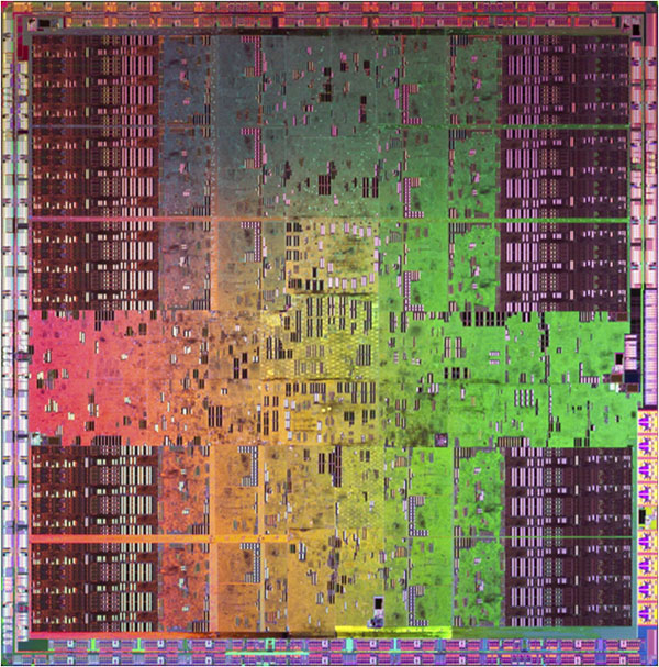
Nvidia's GT200 GPU die shot - Click to enlarge
R600’s seemingly clever design turned out to be an incredible mismatch for the brute that was G80 and it not only underperformed, but also consumed much more power too. The end result was a company that decided to no longer build big GPUs and instead harnessing the sometimes crazed world of multi-GPU technology.
RV670 was a tiny chip in comparison, but delivered roughly the same (and generally slightly more) performance than the product it replaced and that was then followed by R680, the Radeon HD 3870 X2, which was basically a pair of RV670s on one PCB – I’m not quite sure how AMD worked out the maths on the GPU codename, but we’ll run with it anyway.
Just last week, AMD spent time messaging us again on its intentions for the future when it briefed us on its upcoming RV770 graphics chip – only time will tell us if that was a good decision. However, when I spoke to Jen-Hsun Huang, Nvidia’s CEO and President, towards the end of May in Santa Clara, he seemed unfazed by AMD’s decision to no longer make massive chips.
So anyway, we digress – today we’re going to talk about Nvidia’s GT200 chip and the products that will fit under the GeForce GTX 200 series. The GeForce GTX 280 and GTX 260 were announced last week and, together, it’s the first time since November 2006 that the quite simply awesome G80 chip has well and truly ended its tenure at the top of the single GPU pile – it’s time to bid farewell to what has been a fantastic graphics chip.
Because of the amount of things there are to talk about with the GT200 chip, there are going to be several parts to bit-tech’s coverage – today we’re going to spend time looking at the more theoretical side of things and the architecture behind the chip. That will then shortly be followed by our look at gaming performance on both the GTX 280 and GTX 260, and then we’ll see where that takes us.
So, before we get onto the architecture itself, let’s have a look at the hardware...
RELATED ARTICLES


MSI MPG Velox 100R Chassis Review
October 14 2021 | 15:04

Want to comment? Please log in.