
All About Intel Ivy Bridge
Or, everything you need to know, six months before you need to know itIf there’s one thing we love about attending IDF (the Intel Developer Forum) it’s that we usually walk away knowing pretty much everything about a next-gen Intel CPU - from its architecture, through Intel's innovations to reduce its power draw, and even how to overclock the nuts off it. This is the case with Ivy Bridge, Intel’s next-gen LGA1155 CPU family, which we expect to see in March or April of 2012.
There’s been quite a bit of information already released about Ivy Bridge to get up the excitement levels, so we’ll recap all that before diving into the new learnings and their practical implications.
Tri-gate, 22nm transistors
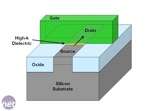
Ivy Bridge will be the first commercial CPU to use Tri-Gate transistors, and also the first to use a 22nm manufacturing process. We’ll borrow Professor Kelin Kuhn’s explanation of a Tri-Gate transistor (mainly because it’s the first explanation we really understood ourselves). The easiest way to think of a Tri-Gate transistor is to imagine a typical transistor as a piece of paper; squish the two sides of it and the middle bows up in the middle, and that’s a 3D transistor, as you can see in the images below.
The easiest way to imagine a Tri-Gate transistor is to think of it as a
normal transistor folded up in the middle
In a typical transistor - referred to these days as a ‘planar’ transistor - only the small layer between the channel and the gate becomes active when the transistor is switched on. This is usually shown in yellow, and is referred to as the dielectric (of high-k fame, in recent transistor manufacturing).
However, in a Tri-Gate transistor, the channel is in three dimensions, meaning that the dielectric around this is also in three dimensions. As electricity can flow around all three sides of the channel, this is a neat way of reducing transistor size on the silicon die (to the width of the fin), while maintaining a sufficiently long gate length for a strong signal.
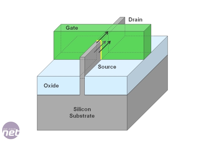
The dielectric of a Tri-Gate transistor is in three planes rather than one
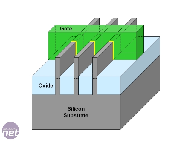
Tri-Gate transistors can be ganged together
Intel didn’t talk too much about this, other than saying it was potentially interesting and useful. We presume that ganged fins can act like fail-safe backups to improve yields of individual dies, or increase bandwidth, or both.
The practical implications are that 3D transistors can either consume 50 per cent less power for the same performance, or deliver 37 per cent more performance for the same power, or some balance of performance and power within those limits.
Is a Tri-Gate transistor just a FinFET?
A Tri-Gate transistor isn’t quite the same as a FinFET transistor, although you're likely to find people use the term FinFET as a generic term for all 3D transistors due to the fin-like look of the transistor channels. Prof Kuhn gave us some specific definitions for various types of 3D transistor - from Pi-Gate to Omega-FET to GAA (Gate-All-Around), each with quirks of design. A FinFET is defined as having a block material across the top of its channel and could therefore be thought of as a dual-gate transistor given the Tri-Gate terminology.
Definitions of fin-like 3D transistors - note the notch on the Omega-FET gates and the
lower gate position in the substrate of the Pi-Gate
Intel has also never claimed to have invented the 3D transistor - Prof Kuhn attributes that honour to Digh Hisamoto’s MuGFET in 1989, with Huang improving on the technique in 1999. Intel didn’t even invent the first tri-gate transistor - Chau and Kavalieros got there first in 2002 and 2006 respectively. What Intel has done, however, is make a viable, cost-effective manufacturing process for microprocessors using Tri-Gate transistors.


MSI MPG Velox 100R Chassis Review
October 14 2021 | 15:04

Want to comment? Please log in.