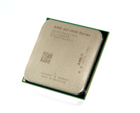
AMD A8-3850 Features
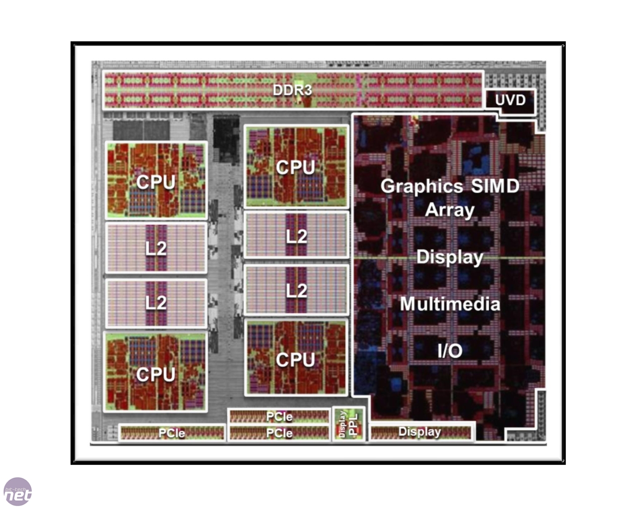
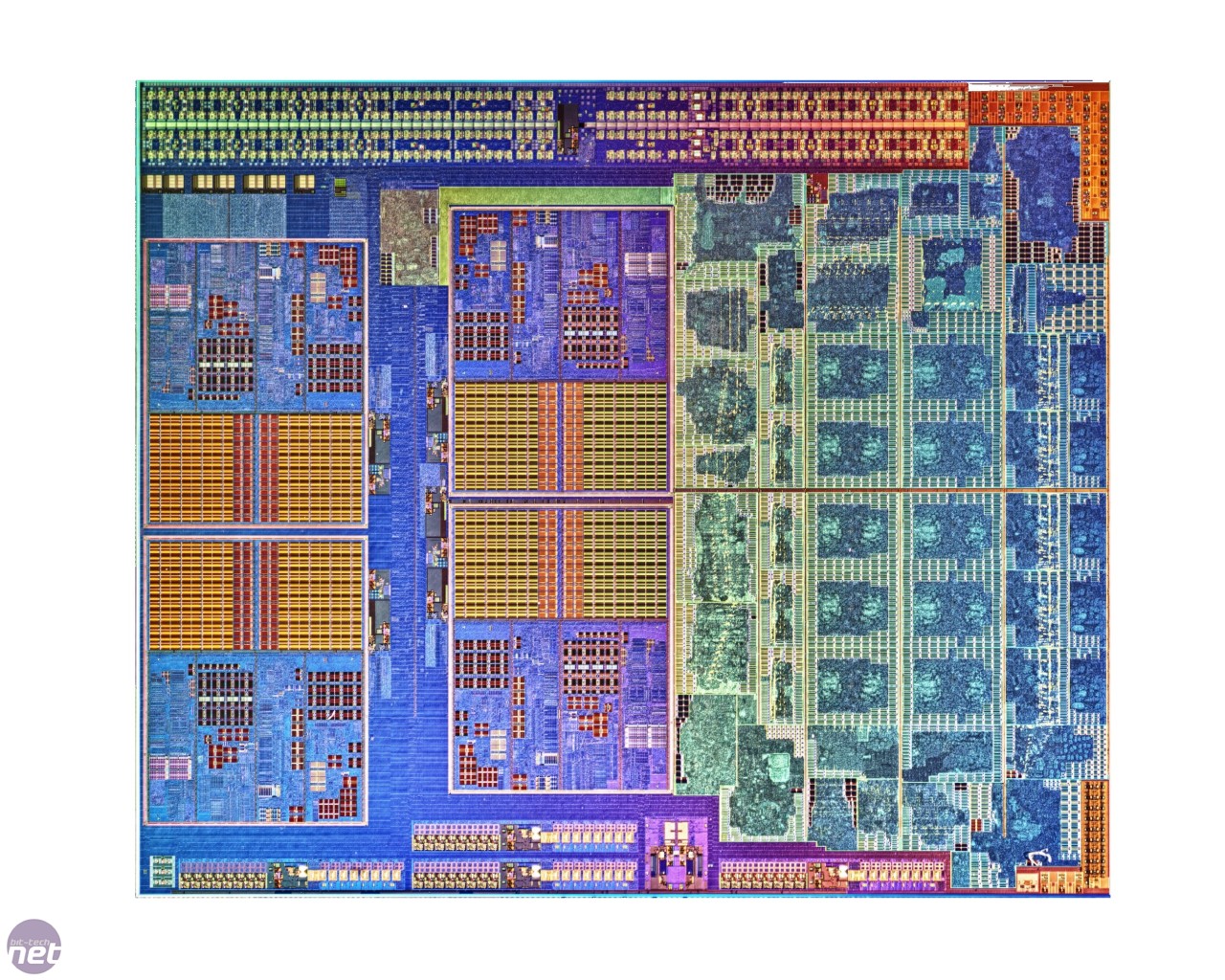
AMD sent us the top-of-the-range A8-3850 APU for testing, which has an MSRP of $135 (we’ve seen it available for pre-order on some sites for around £105), which places it in direct competition with Intel’s dual-core, Hyper Threaded Core i3-2100 (full review to come soon).As we’ve already mentioned, the A8-3850 includes four 32nm Stars-based CPU cores running at a sprightly 2.9GHz. Each core can lay claim to 128KB of Level 1 cache and 1MB of Level 2 cache, although the APU is missing a larger pool of Level 3 cache.
Click to enlarge
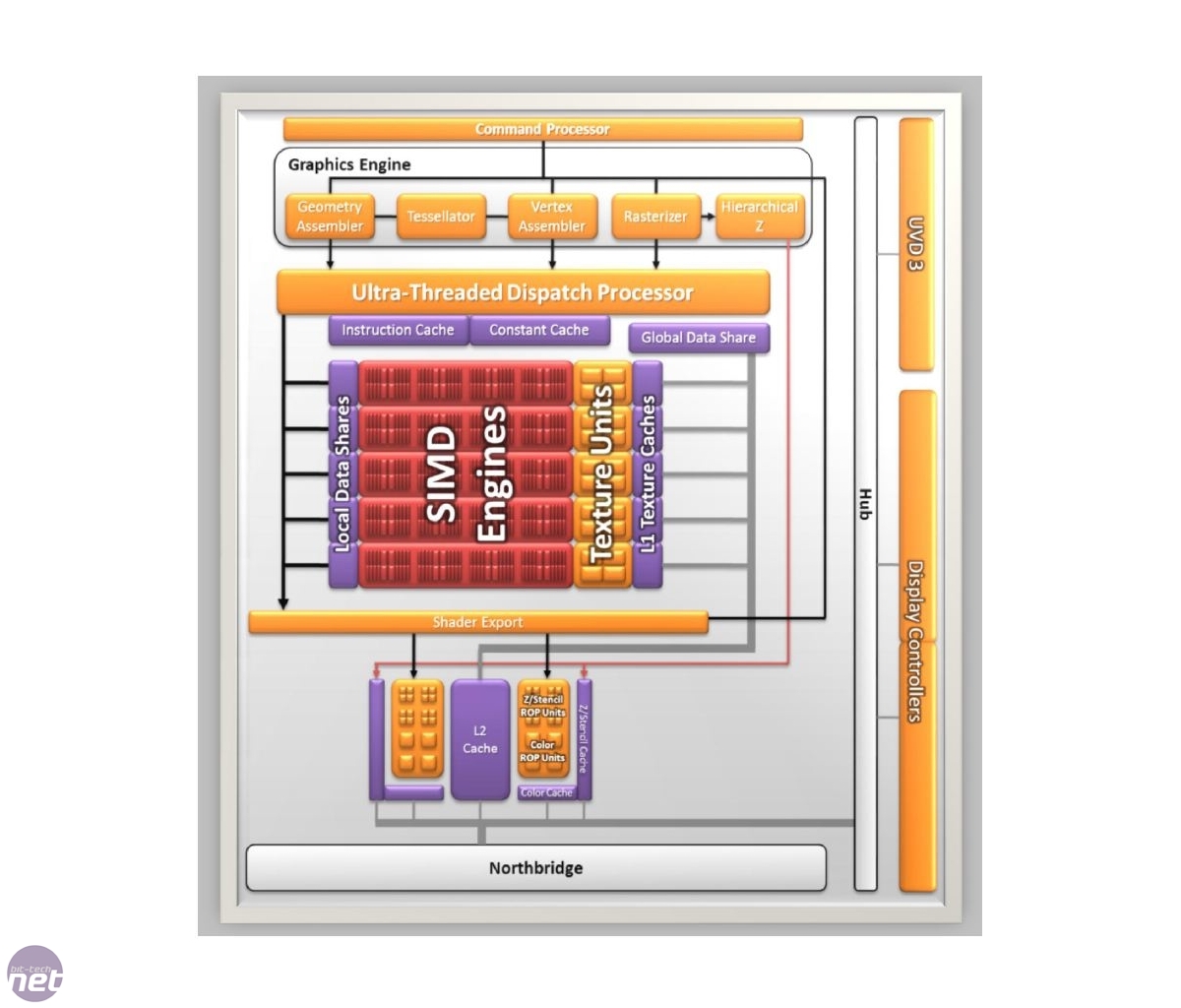
Also tucked under the APU’s integrated heatspreader is a Radeon HD 6550D GPU, which runs at 600MHz. This sounds pretty pedestrian compared to the 850MHz frequency at which the HD Graphics 2000 processor in the i3-2100 runs, but the HD 6550D has a whopping 400 stream processors and 20 texture units, compared to the meagre six execution units of Intel's HD Graphics 2000 processor. The A8-3850 also has the edge over the i3-2100 in terms of features, as the former’s GPU is fully DirectX 11-capable, whereas Intel's graphics processor is only compatible with DirectX 10.
The APU also boasts a number of proprietary AMD features, including the company's Dual Graphics technology. Similar to AMD’s CrossFire technology, this enables the on-board GPU to team up with a discrete AMD GPU to provide extra graphical horsepower.
Click to enlarge
With the Llano architecture, AMD has also debuted asynchronous multi-GPU rendering, enabling different workloads to be distributed to the APU and GPU. At present, only AMD’s low-end discrete GPUs are compatible; these comprise the HD 6670 1GB, HD 6570 1GB, HD 6450 512GB and HD 6350 512MB
AMD A8-3850 Overclocking
As you can see, AMD’s Lynx APUs aren’t targeted at hardcore performance enthusiasts. As a result, we your overclocking options are also a little limited.For example, we were a little dismayed to find out that AMD seems to have taken a leaf out of Intel’s design book by using an integrated clock gen chip. This means that all the clock speeds across the board are tied together. As we’ve seen with Sandy Bridge systems, this setup essentially kills overclocking via the Base Clock (or reference clock when talking about a Llano APU), as increasing this by more than 5 per cent can lead to instability in the SATA and USB sub-systems.
Coupled with the fact that A-series processors are intended to have a locked CPU multiplier, this means that we weren’t very hopeful of pushing our test A8-3850 beyond its stock operating speed of 2.9GHz, based on a reference clock of 100MHz and 29x CPU multiplier.
However, we were intrigued to see that the ASRock A75 Pro4 motherboard we were using for testing allowed us to increase the CPU multiplier to 36x, leading to an overall claimed frequency of 3.6GHz. However, even though CPU-Z did report that the CPU was running at 3.6GHz, the CPU multiplier had not actually changed. In fact, the benchmark results were identical to those at 2.9GHz.
This forced us back to the drawing board, playing with the reference clock to achieve an overclock. As we expected, this proved largely fruitless, as we could only manage a meagre 5MHz overclock to the HT frequency, which pushed the CPU clock to 3.04GHz and the GPU clock to 630MHz.
We spoke to AMD about our overclocking experiences and were told that we’d probably have better experiences with a different motherboard, as some boards have the ability to lock the troublesome SATA and USB clocks to allow more overclocking via the reference clock.
AMD also told us that some boards have invisible dividers that kick in for the SATA and USB clocks at certain reference clock speeds. This could mean that a reference clock of 133MHz results in a stable overclock, whereas a reference clock of 120MHz doesn’t, simply because the higher reference clock has triggered the use of a higher SATA/USB divider. Unfortunately, these tips didn’t help our overclock, as our board resolutely refused to boot at any reference clock above 105MHz.


MSI MPG Velox 100R Chassis Review
October 14 2021 | 15:04

Want to comment? Please log in.