
The pace at which technology is moving these days can be quite frightening – it was only 13 months ago when Intel released its first processor products using the company’s 65 nanometre manufacturing technology. Fast forward to today and Intel has announced that it has made a significant breakthrough in manufacturing technology with the development of high-k, metal gate transistors using its 45 nanometre process node.
Gordon Moore, co-founder of Intel Corporation has stated that “the implementation of high-k and metal materials marks the biggest change in transistor technology since the introduction of polysilicon MOS transistors in the late 1960s.” You would think that was enough to brag about, but Intel doesn’t seem to want to stop there. The company is also bragging about the fact that it has five early-version processors manufactured on the new 45nm process technology up and running in its testing labs.
A couple of days ago, we had the chance to sit down with Intel to discuss the company’s 45 nanometre process node and the next generation multi-core processors that will be manufactured using the technology. Join us as we dive into the process technology advancements behind Intel’s second-generation products based on the Core microarchitecture.
On Intel’s 65 nanometre process, gate dielectric walls are 1.2 nanometres thick – that’s equivalent to five atomic layers across, if we put things into perspective. This essentially means that Intel’s processor engineers are designing chips on an almost atomic structure level, and shrinking current silicon dioxide gate dielectric walls even further would exaggerate this even further.
Obviously, this has some potentially quite serious implications, because gate leakage tunnelling through the silicon dioxide increases exponentially when the dielectric gate walls get thinner and thinner. Excessive current leakage causes an increase in power dissipation and heat output – something that the Prescott core was famous for. What you end up with is a transistor that’s never fully switched to off; instead, you’ve got millions of transistors that resemble a light bulb that only dims when you switch it off. In other words, the transistors end up becoming power inefficient.
 Even if current leakage wasn’t a problem, Intel would have run into other problems. This is because the dielectric wall in a 65 nanometre CMOS transistor gate is so thin – Intel is simply running out of atoms. With energy efficiency becoming more and more important to end users (and our planet), something needed to be done because the problems imposed a practical limit on the extensibility of Moore’s Law.
A few years ago, Intel’s advanced R&D teams set about designing and engineering the next generation of transistor technology so that the chip giant could continue to drive chip technology forwards at an exponential rate. Here’s where high-k metal gate transistors come into play.
Gordon Moore, co-founder of Intel Corporation has stated that “the implementation of high-k and metal materials marks the biggest change in transistor technology since the introduction of polysilicon MOS transistors in the late 1960s.” You would think that was enough to brag about, but Intel doesn’t seem to want to stop there. The company is also bragging about the fact that it has five early-version processors manufactured on the new 45nm process technology up and running in its testing labs.
A couple of days ago, we had the chance to sit down with Intel to discuss the company’s 45 nanometre process node and the next generation multi-core processors that will be manufactured using the technology. Join us as we dive into the process technology advancements behind Intel’s second-generation products based on the Core microarchitecture.
Running out of atoms...
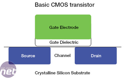
According to Moore’s Law, the transistor density on integrated circuits doubles roughly every two years – this has been the case for well over 40 years now. Over the last 15 years or so, Intel has used a silicon dioxide (SiO2) gate dielectric inside its transistors, but the improvements made in process technology has meant that gate dielectric walls have become much thinner. For those not familiar with the terminology, gate dielectric is a fancy term for an insulator, designed to prevent current leakage between the electrode and the source and drain (see diagram below).On Intel’s 65 nanometre process, gate dielectric walls are 1.2 nanometres thick – that’s equivalent to five atomic layers across, if we put things into perspective. This essentially means that Intel’s processor engineers are designing chips on an almost atomic structure level, and shrinking current silicon dioxide gate dielectric walls even further would exaggerate this even further.
Obviously, this has some potentially quite serious implications, because gate leakage tunnelling through the silicon dioxide increases exponentially when the dielectric gate walls get thinner and thinner. Excessive current leakage causes an increase in power dissipation and heat output – something that the Prescott core was famous for. What you end up with is a transistor that’s never fully switched to off; instead, you’ve got millions of transistors that resemble a light bulb that only dims when you switch it off. In other words, the transistors end up becoming power inefficient.
A few years ago, Intel’s advanced R&D teams set about designing and engineering the next generation of transistor technology so that the chip giant could continue to drive chip technology forwards at an exponential rate. Here’s where high-k metal gate transistors come into play.
RELATED ARTICLES


MSI MPG Velox 100R Chassis Review
October 14 2021 | 15:04

Want to comment? Please log in.