
Gate First vs Gate Last
One key area that differentiates the 28nm technology is the 'gate first' versus 'gate late' in high-k Metal Gate manufacturing.It's pretty much split the industry in two, with Global Foundries and its development partners; IBM, Toshiba, Infineon, ST Micro and Samsung (to name a few), sticking to a traditional gate first approach. Last summer TSMC changed its mind to follow in Intel's 'gate-last' wake as well (as Intel used high-k Metal Gate first on 45nm).
Intel has also been very vocal about is its use of 'gate last' high-k MG. The company cites that because of the high temperature processes needed during high-k MG manufacture, this causes yield issues or very complex manufacturing to work around when making the temperature sensitive transistor gate first. Intel backs up this claim with the statement that its '45nm P1266 process now represents Intel's highest yielding process ever' (Page 3 of its White Paper).
The problem is, a 'gate last' process requires a redesign of the layout and process technology; it's reported TSMC had to have 'face to face meetings' with its customers to get them on board - so it costs more for all parties, even if it is more reliable. However, considering the serious yield issues TSMC has faced at 40nm we wouldn't have thought its customers needed much convincing.
Its Chairman and CEO, Morris Chang, predicts the entire industry will eventually have to use the 'gate last' method, stating,
"I do believe the 'gate first' people will change to 'gate last' at the 22 nm node," he said.
"I am not criticizing them, but I think they will change. Unless they can find some very innovative way to adjust the threshold voltage without a lot of high cost, they will have to change."
Global Foundries has similar customer demands to TSMC, but the company appears to have taken the decision to stick with gate first and manage the yields the best it can for now. The question being, will it be a gamble that pays off? For AMD in particular, it certainly needs it to.
Nvidia's CEO famously claimed he never paid for bad parts from TSMC when it had 40nm yield problems, and we have to wonder whether Global Foundries is offering the same deal if its 32nm and 28nm yields suffer the same. Our negativity was further impacted because not once did Global Foundries put an actual number to its yields, despite the fact its 32nm process should be approaching production readiness.
Second Generation Immersion EUV Lithography
Back to fundamentals now: to make the electronic grid on a silicon wafer a visual mask is made, and then 'light' shone onto it to etch away the bits which aren't covered. However, as transistor gate lengths get ever smaller, finding a wavelength of radiation short enough to erode the chemicals left bare between the tiny masks is getting ever more difficult.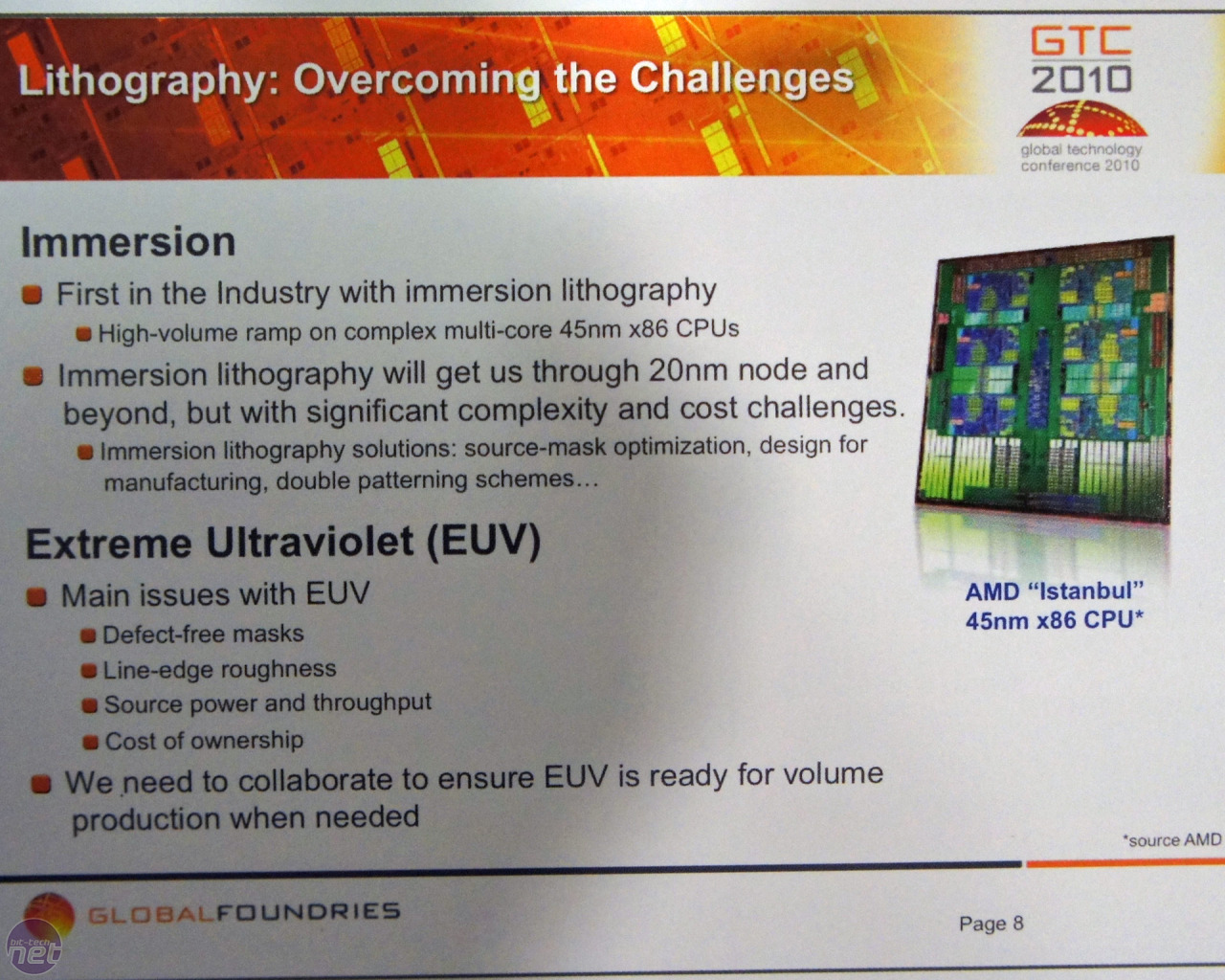
Click to enlarge
Visual light only ranges from a lazy red at 780nm down to an energetic blue-violet at 380nm, but going further beyond blue into the ultra-violet spectrum we eventually hit a high powered 'extreme UV' at 193nm. This is already in use on the more recent generations of CPUs and GPUs. More recently, additional techniques such as double-patterning have been required, but this causes a large increase in fabrication costs. AMD is using an alternative route called immersion EUV lithography, where the mask and wafer are put under a liquid (usually water) rather than left open to air. That liquid has a greater refractive index than air (water = 1.44) and is used as a lens to further focus the radiation, providing a 30-40 per cent clearer image, which goes some way to better overall chip yields.
Global Foundries has already premièred its mass production immersion lithography to make AMD's Istanbul 45nm 6-core CPU earlier this year and will continue to learn from these experiences when it launches its 32nm 'second generation' in 2011. In its slides the company claims its 'First in the industry', however that depends on which competitors Global Foundries has included.
Intel was already shipping 32nm x86 hardware a few months before Istanbul arrived - not to mention 34nm NAND parts since way back in 2008. Intel is also due to ship 25nm NAND using immersion lithography within the next few months too - again, ahead of Global Foundries 32nm production of AMD's Llano in the first half of next year.
Then there's also TSMC, which, according to reports has been using immersion techniques in technical demonstrations since 90nm and 65nm. So while we're finding it difficult to determine which products exactly received immersive treatment, it's highly likely that as a competing fab to Global Foundries, TSMC is also ahead of the game.
However, TSMC doesn't make x86 parts (until Bobcat in December) and Intel doesn't take external customers for CPU manufacturing, so, yes, Global Foundries might technically be a 'first in the industry'.
RELATED ARTICLES


MSI MPG Velox 100R Chassis Review
October 14 2021 | 15:04

Want to comment? Please log in.