The Fermi architecture – a quick overview
Nvidia has designed its new Fermi architecture around tessellation, which is the most important feature of DX11. Tessellation is the process of taking simple geometry and adding more complexity and detail on-the-fly, and the process aims to eliminate angular silhouettes for game objects (from guns and crates to faces and plants) and also to smooth out the jarring effect of LODs (levels of detail), where the extra information and detail needed to make objects look more realistic close up is manually specified by the developer and is added by the game to objects as you approach them.Added to this is the benefit of geometrically richer surfaces which will reduce the need to use bump maps and parallax occlusion maps to trick the eye into thinking a surface is rough rather than entirely flat.
Developers should also benefit from tessellation, as it will reduce the need to create tiresome LOD libraries - instead a developer can just attach some tessellation parameters to each model. It’s notable that we’ve already seen a few DX11-compatible games which use tessellation – in fact, there are probably more DX11-compatible games now (only five months after DX11 was released with Windows 7) then there were DX10 games after a year of Vista being on sale.
The challenge that tessellation brings to GPU design is that it’s increasing the amount of geometry work that a GPU has to perform. While pixel shading hardware and performance has increased exponentially over the last five years, we’ve not seen much in the way of geometry (vertex) performance improvements. The front-end of GPUs, which is the stage at which geometry and vertices is handled, hasn’t evolved much at all in recent years.


The benefits of tessellation are fairly clear, and the potential huge. Click to enlarge.
Nvidia has chosen a much different route to that of ATI to implement tessellation. While ATI’s implementation is fairly simple – it’s beefed up the front-end of Cypress to have a tesselator feeding two rasteriser units – Nvidia’s Fermi design has 16 tesselator units and four rasterisers distributed throughout the GPU. Whether these units have the same power and capabilities as the units of ATI’s Cypress remains to be seen (we’re still doing our in-depth testing, and will bring you the results soon).
A Distributed, Modular Design
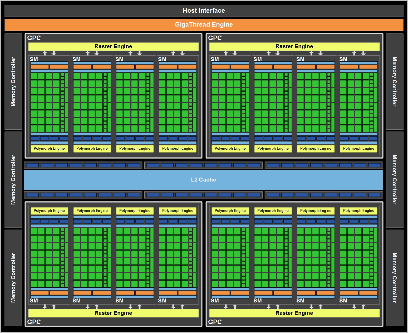
Nvidis's Fermi architecture. Click to enlarge
If you’ve never heard of Raster or Polymorph Engines, that’s fine, because they’re new. It’s these two new types of engines (or rather, it’s the division of their capabilities) that’s the real innovation of Fermi. Previously a GPU would have a large unit that did vertex fetching, triangle assembly and rasterisation, but Nvidia says that this kind of arrangement would lead to unacceptable stalls if tessellation was introduced.
The issue is that if you tessellate, you need to feed the outputs of that work back into the monolithic front-end, which would become a bottleneck (or, if it received significant upgrades, would be frequently under-used, and therefore an expensive waste of transistors). With more redundancy built into the system, tessellation can occur without stalling other tasks.
The problem of potential under-utilisation has, Nvidia claims, been largely avoided by Fermi’s ability to process two kernels simultaneously – it’s a MIMD (Multiple Instruction, Multiple Data) design. This means that the GPU doesn’t have to wait for the last little bit of task A to complete before it start flooding unused parts of the GPU with task B. If there’s work to be done, and if there’s resources in the GPU to do that work, it won’t have to wait. This ability could help a single Fermi GPU to run PhysX or GPU-based AI as well as conventional rasterisation graphics without stuttering.
Specifications
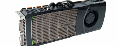
The Fermi architecture has 512 stream processors (which Nvidia refers to as ‘CUDA cores’), arranged into 16 clusters, or SMs (Streaming Multiprocessor). Each SM has a PolyMorph Engine, and there are four SMs per GPC. Each GPC can access the 768KB of Level 2 cache that runs through the centre of the GPU via the 48 ROPs. Fermi has a 384-bit GDDR3 memory controller, meaning that full-fat Fermi cards will have 1.5GB of memory.At launch there are two versions of Fermi card, the GeForce GTX 470 and GeForce GTX 480. Neither card uses the full 512 stream processors, and while the GTX 480 has the full 384-bit memory bus and 1.5GB of 924MHz GDDR5 (3.7GHz effective) for 177GB/sec of memory bandwidth. The GTX 470 has only a 320-bit bus and GDDR5 memory that runs at 837MHz (3.3GHz effective) for 134GB/sec of memory bandwidth.
Specifications | ||||
| Nvidia GeForce GTX 480 | Nvidia GeForce GTX 470 | ATI Radeon HD 5870 | ATI Radeon HD 5850 | |
| Stream processors | 480 | 448 | 1,600 | 1,440 |
| Frequency (core) | 700MHz | 607MHz | 850MHz | 725MHz |
| Frequency (SPs) | 1,401MHz | 1,215MHz | 850MHz | 725MHz |
| Manufacturing process | 40nm | 40nm | 40nm | 40nm |
| Texture units | 60 | 56 | 80 | 72 |
| ROPs | 48 | 40 | 32 | 32 |
Memory | ||||
| Memory | 1,536MB GDDR5 | 1,280MB GDDR5 | 1GB GDDR5 | 1GB GDDR5 |
| Memory Frequency | 924MHZ (3.7GHZ, effective) | 837MHz (3.3GHz, effective) | 1.2GHz (4.8GHz, effective) | 1GHz (4GHZ, effective) |
| Memory interface | 384-bit | 320-bit | 256-bit | 256-bit |
| Memory Bandwidth | 177GB/sec | 134GB/sec | 154GB/sec | 128GB/sec |
Ports and Power | ||||
| Connections | 2 x dual-link DVI, 1 x mini-HDMI, 2 x SLI | 2 x dual-link DVI, 1 x mini-HDMI, 2 x SLI | 2 x dual-link DVI, 1 x DisplayPort, 1 x HDMI, 2 x CrossFire | 2 x dual-link DVI, 1 x DisplayPort, 1 x HDMI, 2 x CrossFire |
| Power inputs | 6-pin PCI-E + 8-pin PCI-E | 2 x 6-pin PCI-E | 2 x 6-pin PCI-E | 2 x 6-pin PCI-E |
| Idle Board Power | Unspecified | Unspecified | 27W | 27W |
| Max Board Power | 250W | 215W | 188W | 151W |
| Recommended PSU | 600W | 550W | 500W | 500W |
We'll bring you an in-depth analysis of the Fermi architecture soon, and will also delve into whether Nvidia's implementation of tessellation gives it greater potential than ATI's Cypress design. This review focuses entirely on real-world game performance.
RELATED ARTICLES


MSI MPG Velox 100R Chassis Review
October 14 2021 | 15:04

Want to comment? Please log in.