
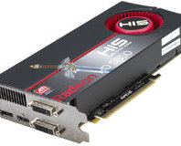
ATI Radeon HD 4850 512MB reference card
Core Clock: 625MHzMemory Clock: 2,000MHz (effective)
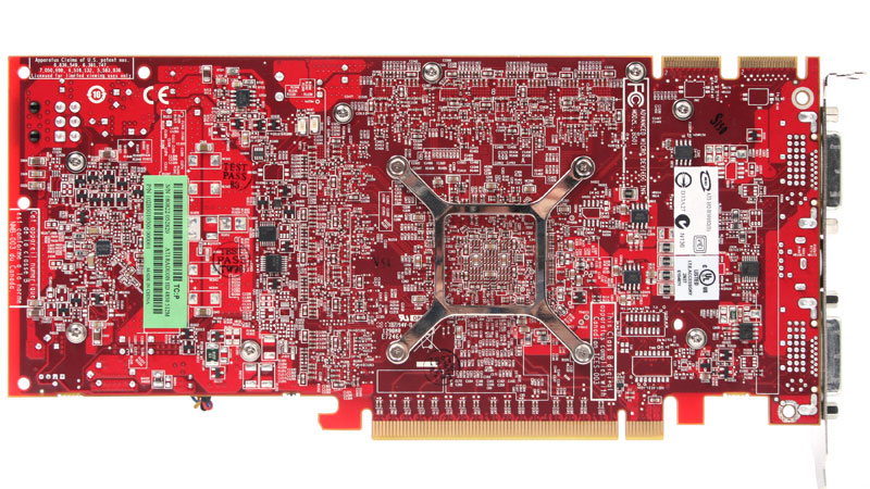
AMD's ATI Radeon HD 4850 512MB reference card looks very similar to the Radeon HD 3850 card it is replacing. The differences between the two are very subtle from a distance, but they're a lot more obvious as soon as you get up close and personal.
The first thing to notice is that the Radeon HD 4850 is about 4mm longer than the HD 3850 at 234mm and then upon closer inspection, you'll realise that the capacitor layout and supplementary power connector placement have changed as well.
Looking at the back of the PCB, you can see that ATI has changed the memory layout – it's no longer a horseshoe and the eight chips are instead laid out in an L-shape. Removing the heatsink confirms that this is the case – the card uses eight 64MB Qimonda 1.0ns GDDR3 memory chips, meaning there's a total of 512MB of on-board memory. These are rated to 1,000MHz (2,000MHz effective) and AMD has set the reference clock for them at their rated speed on the Radeon HD 4850.

Click to enlarge
Interestingly, they've been rotated by 90 degrees on the 4850, so the broad edge of the DRAM chip is now parallel with the GPU's substrate packaging – this means there's a little bit more space in between the DRAMs and the power phases. And while we're talking about power delivery, nothing much has changed on the GPU front. There are still four slimline chokes and eight Power-Pak MOSFETs (four per phase, two chokes per phase, two phases in total) delivering power to the RV770 core.
However, things have been changed slightly for the memory. There is still a single power phase (with one choke and two Power-Pak MOSFETs), but the old 'open' choke has now been replaced with the same type of choke used for the rest of the card’s power phases, although its markings are different.

Click to enlarge
With all of this in mind, it’s no surprise that AMD hasn’t changed the way power is delivered to the card. By default, 75W of the board’s power is supplied via the PCI-Express interconnect in order to retain backwards compatibility with older motherboards but on newer, PCIe 2.0 boards, you can adjust this in your motherboard BIOS. However, even despite this, the six-pin PCI-Express power connector needs to be connected at all times because the card’s maximum power draw is quoted at 110W. With all of this in mind, there should be more than enough power available for some healthy overclocking headroom.
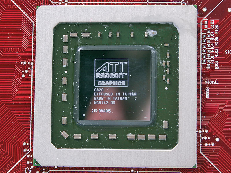
On the Radeon HD 4850, the RV770 GPU is clocked conservatively at just 625MHz, which means it’s no surprise to see that the heatsink design is almost identical to the one used on the Radeon HD 3850. That said, there have been a few refinements made in the eight months between the two cards’ release dates.
RELATED ARTICLES


MSI MPG Velox 100R Chassis Review
October 14 2021 | 15:04

Want to comment? Please log in.