
RV670 - almost all of R600 (and more) at half the size...
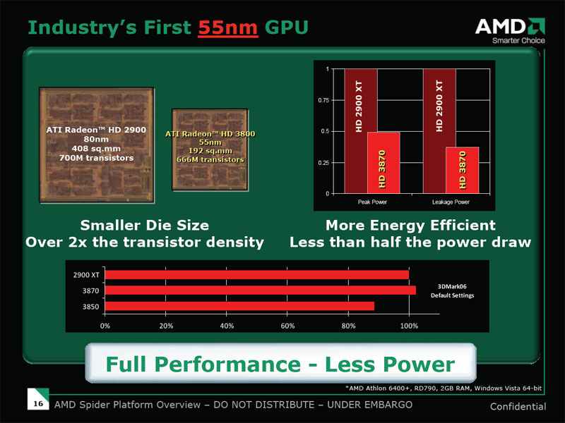
The Radeon HD 3800-series is based on AMD’s RV670 graphics processor. The architecture behind this chip is largely the same as the one behind the R600 chip for which it is replacing, but that’s not to say there haven’t been some changes made.AMD took a risk with RV670, as it is the first GPU to be manufactured using a 55nm process node. In the case of RV670, AMD has utilised TSMC’s 55GT process node – the most cost effective of the 55nm processes which Taiwan Semiconductor Manufacturing Corp offers.
In reality, it wasn’t quite as big of a risk as one would first think. The reason I say this is that AMD has taken a familiar architecture, made a few enhancements and tweaks and then implemented it onto a new process node – this is something that Intel is doing with its CPUs in the tick-tock movement every other year. The 55nm process is an optical shrink of the more commonly-used 65nm process, which AMD is already familiar with as its RV630 and RV615 GPUs were fabbed on one of TSMC’s 65nm processes.
As a result of the process shrink, RV670 is a pretty small GPU by today’s standards, measuring up at just 192mm² and in that space there are only 666 million transistors. In comparison, R600 was a 700-million transistor monster which measured up at 408mm² – more than double RV670’s surface area. There’s a number of reasons for R670 being so much smaller, which we’ll outline over the course of this GPU analysis.
Shader core:
First and foremost, there are a total of 64 five-way superscalar shader processors or 320 stream processors if you want to talk in terms of execution units. These shader processors are arranged into four SIMD units with each one containing sixteen shader processors, or 80 stream processors.This all sounds pretty familiar, right?
The reason it sounds familiar is that RV670 is a superset of R600 in terms of features - there are some differences, but they’re subtle. For example, the subtlety in RV670’s shader core is that AMD has added support for DirectX 10.1 into the equation. We’ll come back to DirectX 10.1 in more detail in a couple of pages, but it’s the most important overhaul in the shader core and in simple terms, it helps to standardise a lot of the features that didn’t quite make it into DirectX 10.
Of the five instruction units in each superscalar shader processor, there are four units which can handle a limited number of instructions (FP MAD, FP MUL, FP and INT ADD along with dot product calculations too) per clock cycle. RV670 adds in double precision capabilities which can be done at quarter speed, although there’s no exposure for this in current 3D graphics APIs. For what it’s worth, it’s exposed via AMD’s CTM SDK and therefore can be used for GPGPU workloads.
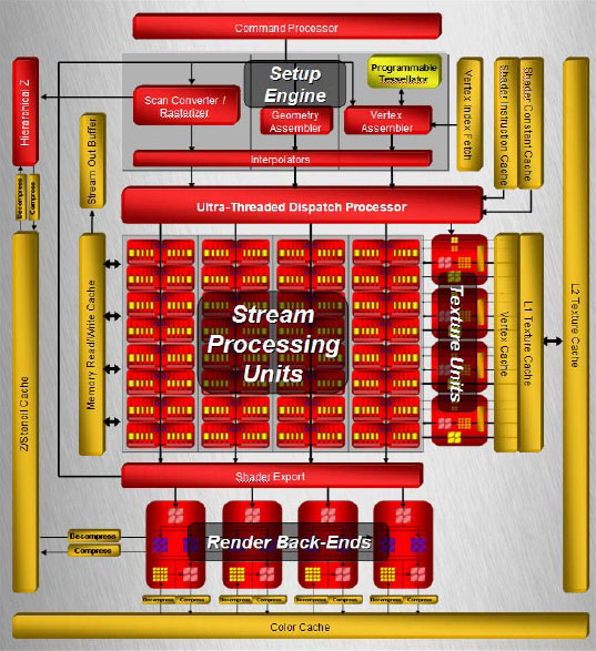
RV670 flow diagram - it looks familiar, doesn't it?
The fifth unit in each shader processor can’t handle dot products, integer ADD commands or double precision, but can handle more types of instructions than the thinner units – these include things like integer multiply and division, along with bit shifting, and transcendental commands like SIN, COS, LOG, and so on. All of the shader operations are done with 32-bit precision.
Additionally, there’s also one final ALU in R600/RV670 shader processor design, on top of the five shader units. This is used for branch execution, which means it handles flow control and conditional operations. Back when AMD launched R600, it said that this unit would almost eliminate the flow control performance overheads.
RELATED ARTICLES


MSI MPG Velox 100R Chassis Review
October 14 2021 | 15:04

Want to comment? Please log in.