
Conventional Transistor Designs:
Aside from the obvious improvements in manufacturing technology and miniaturisation, there have only been minor refinements to the CMOS transistors inside a modern CPU. Of course, that is until Intel introduces processors based on its new 45nm process. Before we get to that though, let’s go back through time for a bit of a history lesson.Ever since the late 1960s, transistors have been made of a basic selection of materials. Using the simplified diagram on the previous page as an example, the gate electrode was made out of polysilicon, while the gate dielectric was of course silicon dioxide. Inside the transistor itself, the source and drain are made using doped silicon, while the channel area between the source and drain is where the current flows.
By the 1980s, manufacturing process technology had improved exponentially in accordance with Moore’s Law and there was a need to refine the transistor design a little in order to improve transistor performance. What Intel opted to do was to keep the remainder of the transistor construction the same as it was previously, but in addition, the chip giant’s engineers added a low resistance capping layer. This refinement helped to reduce current leakage back down to a low level when the transistor was switched off, while still enabling the current flow from source to drain to be as high as possible when the transistor was switched on.
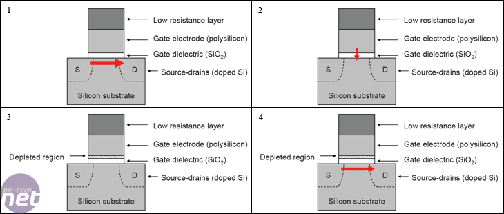
When this happens, the numbers of conducting carriers will be severely reduced in a thin region at the bottom of the polysilicon electrode gates. This causes an unexpected increase in the thickness of the gate dielectric which then causes problems in the transistor because the on current depreciates, while the off current increases significantly.
High-k, Metal Gate Transistors:
In order to solve these problems, Intel has replaced the silicon dioxide used in the gate dielectric with a thicker hafnium-based high-k material. The company claims that this reduces the current leakage by more than ten times over the silicon dioxide that was used in the past.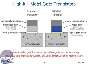
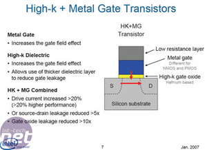
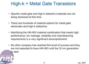
This, in conjunction with the high-k gate dielectric, has given Intel more than a 20% increase in transistor performance while reducing the source-to-drain leakage by more than five times, improving energy efficiency inside each transistor. The smaller, more energy efficient transistors also require less energy to switch on and off and have reduced active switching power consumption by close to 30%.
RELATED ARTICLES


MSI MPG Velox 100R Chassis Review
October 14 2021 | 15:04

Want to comment? Please log in.