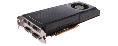
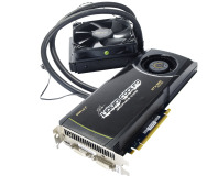
GeForce GTX 580 Specifications
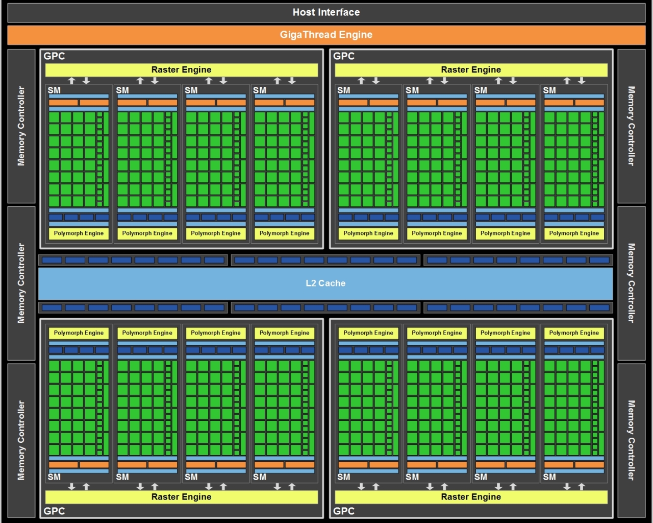
The GeForce GTX 580 1.5GB uses all 16 SMs
However, the new GF110 design still uses the 32 stream processors per SM layout of the original GF100 rather than the 48 per SM of the GeForce GTX 460 GPU.
Even Nvidia sees the 32 layout as a less efficient design, but we suspect that it’s not possible to get four GPCs (Graphics Processing Clusters) with four SMs each onto a die small enough to actually make if each SM contained 48 stream processors rather than 32. In the end, brute force wins out.
Perhaps this layout will change with TSMC’s 28nm process, but that’s not due until halfway through 2011, with GPUs based on this process (from ATI and Nvidia) pencilled in for the autumn of that year.
As well as the extra resources, and the increased high-precision fp16 capabilities (which Nvidia claims is worth a 4-12 per cent performance increase), the GeForce GTX 580 1.5GB operates at higher frequencies than the GeForce GTX 480 1.5GB. While the GPU core of the latter runs at 700MHz (meaning that its 480 stream processors operate at 1.4GHz) the GPU core of the GeForce GTX 580 1.5GB runs at 772MHz, with its 512 stream processors clocked at 1.544GHz.
The 1.5GB of GDDR5 memory also runs faster, with an effective frequency of 4.08GHz rather than 3.7GHz. While this gives the GTX 580 1.5GB more memory bandwidth, the rest of the GPU is the same, with the same 384-bit memory interface and 48 ROPs. The reason for the rise in texture units (from 60 to 64) is because each SM of the GF100 design contains four texture units - unlocking the 16th SM unlocked four more textures.
| Nvidia GeForce GTX 580 1.5GB | Nvidia GeForce GTX 480 1.5GB | Nvidia GeForce GTX 470 1,280MB | ATI Radeon HD 5870 1GB | ATI Radeon HD 6870 1GB | ATI Radeon HD 5970 2GB | |
| GPU | ||||||
| Codename | GF110 | GF100 | GF100 | Cypress XT | Barts XT | Hemlock XT |
| Frequency | 772MHz | 700MHz | 607MHz | 850MHz | 900MHz | 725MHz |
| Stream Processors | 512 (1,544MHz) | 480 (1.4GHz) | 448 (1,215MHz) | 1,600 (850MHz) | 1,120 (900MHz) | 2 x 1,600 (725MHz) |
| Layout | 16 SMs, 4 GPCs | 15 SMs, 4GPCs | 14 SMs, 4 GPCs | 20 SIMD engines | 14 SIMD engines | 2 x 20 SIMD engines |
| Rasterisers | 4 | 4 | 4 | 2 | 2 | 2 x 2 |
| Tesselation Units | 16 | 15 | 14 | 1 | 1 | 2 x 1 |
| Texture Units | 64 | 60 | 56 | 80 | 56 | 2 x 80 |
| ROPs | 48 | 48 | 40 | 32 | 32 | 2 x 32 |
| Transistors | 3 billion | 3 billion | 3 billion | 2.15 billion | 1.7 billion | 2 x 2.15 billion |
| Size | 530mm2 | 530mm2 | 530mm2 | 334mm2 | 255mm2 | 2 x 334mm2 |
| Process | 40nm | 40nm | 40nm | 40nm | 40nm | 40nm |
| Memory | ||||||
| Amount | 1.5GB GDDR5 | 1.5GB GDDR5 | 1,280MB GDDR5 | 1GB GDDR5 | 1GB GDDR5 | 2 x 1GB GDDR5 |
| Frequency | 1.02GHz (4.08GHz effective) | 924MHz (3.7GHz effective) | 837MHz (3.2GHz effective) | 1,050MHz (4.2GHz effective) | 1,050MHz (4.2GHz effective) | 1GHz (4GHz effective) |
| Interface | 384-bit | 384-bit | 320-bit | 256-bit | 256-bit | 2 x 256-bit |
| Bandwidth | 192.4GB/sec | 177GB/sec | 134GB/sec | 134.4GB/sec | 134.4GB/sec | 2 x 128GB/sec |
| Card Specifications | ||||||
| Power Connectors | 1 x 6-pin, 1 x 8-pin PCI-E | 1 x 6-pin, 1 x 8-pin PCI-E | 2 x 6-pin PCI-E | 2 x 6-pin PCI-E | 2 x 6-pin PCI-E | 1 x 6-pin, 1 x 8-pin PCI-E |
| Maximum Power Draw | 244W | 250W | 215W | 188W | 151W | 294W |
| Idle Power Draw | Unspecified | Unspecified | Unspecified | 27W | 19W | Unspecified |
| Recommended PSU | 600W | 600W | 550W | 500W | Unspecified | Unspecified |
| Typical Street Price | £400 | £330 | £200 | £320 | £220 | £490 |


MSI MPG Velox 100R Chassis Review
October 14 2021 | 15:04

Want to comment? Please log in.