Nvidia GeForce GTX 680 2GB Review
Manufacturer: Nvidia
UK Price (as reviewed): £429 (inc VAT)
US Price (as reviewed): $499 (ex TAX)
It’s funny how history tends to repeat itself. Two years ago, almost to the day, Nvidia released its first DX11 GPU based on the Fermi architecture, the GTX 480 1.5GB. Shipping six months after AMD had debuted its DX11 GPUs based on the very successful Evergreen architecture, Nvidia was left playing catch up with a card that failed to impress. Fast forward to 2012 and we again find Nvidia trailing AMD.
The HD 7900 series of graphics cards and their 28nm Tahiti GPUs have been on sale for close to three months, with AMD filling out the rest of its range in the meantime to greater (HD 7800 series) and lesser (HD 7700 series) success. Today sees the first answering shot from Nvidia in the battle for 28nm supremacy, with the flagship GTX 680 2GB taking aim at AMD’s high-end. Can Nvidia banish the Fermi-flavoured demons of 2010 and deliver a GPU to be proud of? Let’s find out.
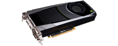
Click to enlarge - Will the GTX 680 2GB be your next graphics card upgrade?
Nvidia is calling the Geforce GTX 680 2GB the fastest, most efficient GPU ever built; bold claims considering the substantial increases on both fronts exhibited by AMD’s 7-series graphics cards. There’s a lot of new technology, design choices and features to cover, so we’ll try and hit the basics on this page, before going into (a lot) more detail separately.
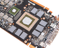
The 28nm Kepler GPU at the heart of the GTX 680 2GB has been dubbed GK104 by Nvidia. It’s a 3.54 billion transistor chip, with a die size of 294mm²; in comparison to the GTX 580 1.5GB’s GF110 GPU, that has 18 per cent more transistors in a 40 per cent smaller die. In comparison, AMD’s Tahiti XT is much larger, cramming 4.3 billion transistors into a 365mm die.
Kepler’s design retains some elements of the Fermi architecture, whilst significantly updating parts such as the SM design. The result is a stream processor count of 1,536, triple that of the GTX 580 1.5GB, but with a unified clock speed. Yes, the shader clock has finally died. This means that despite tripling the steam processor count, the GTX 680 2GB’s stream processors run 35 per cent slower than those of the GTX 580 1.5GB.
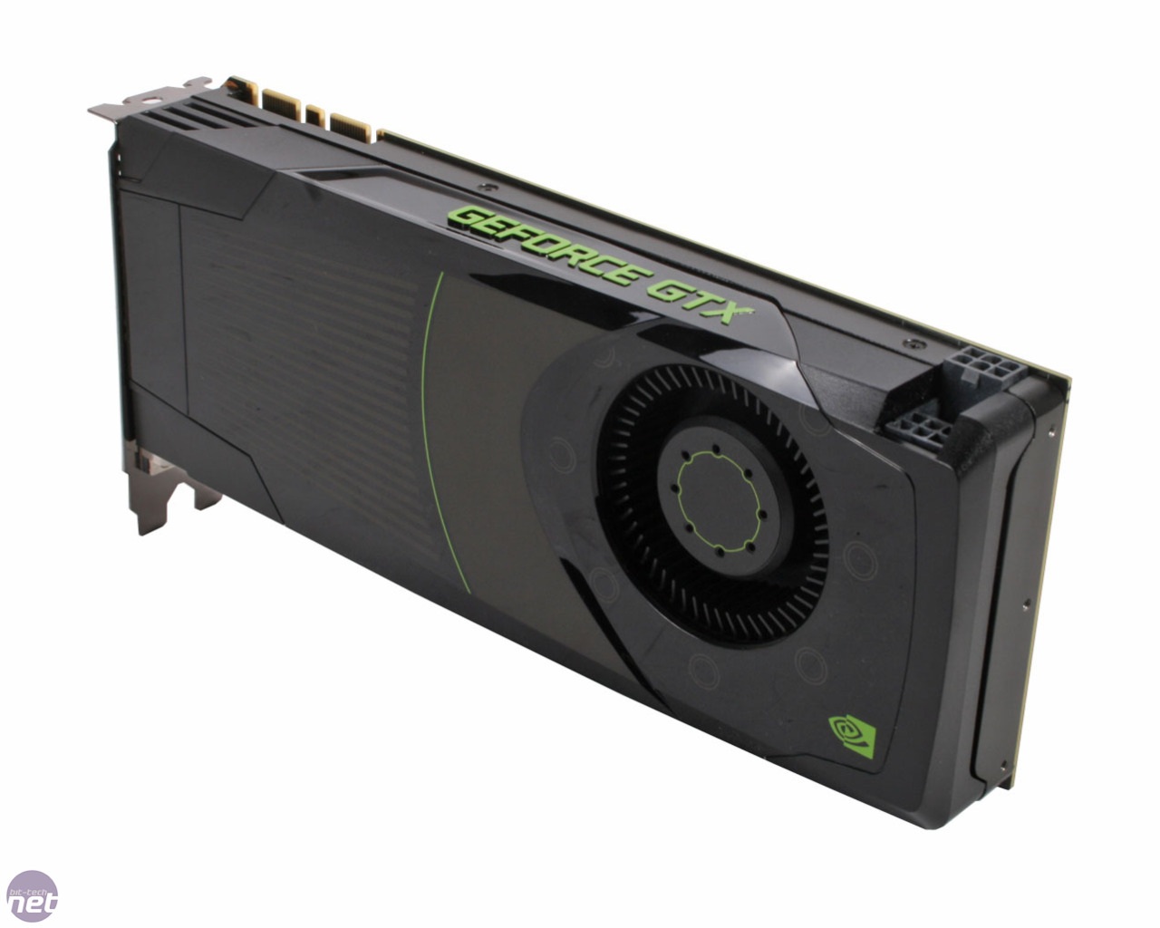
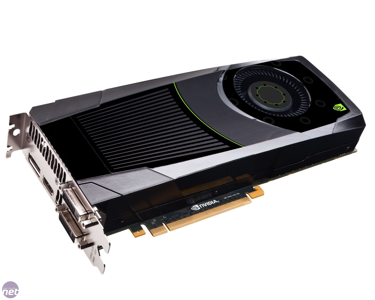
Click to enlarge
Elsewhere, the GTX 680 2GB offers a 256-bit memory interface, with its GDDR5 running at a blistering 1.5GHz (6GHz effective). The memory interface is actually a reduction from the GTX 580 1.5GB though, which, like the HD 7970 3GB, boasts a 384-bit interface. The result is that the GTX 680 2GB’s 192.26GB/sec of memory bandwidth is slightly less than the GTX 580 1.5GB’s 192.4GB/sec, but some way behind the HD 7970 3GB’s 264GB/sec.
Despite a small step backward when it comes to effective memory bandwidth, the card’s core clock speed sees a significant new technology in the form of GPU Boost. We’ll explain it in greater detail later, but the technology, similar in concept to Intel’s Turbo Boost, results in a GPU that runs at a minimum clock speed of 1,006MHz, with the potential for a stock card to be boosted up to 1,110MHz under the right graphical loads.
With even the lowest core clock speed a 30 per cent increase over that of the GTX 580 1.5GB and the net through-put improvement from the new approach to stream processors, there’s clearly a great deal of performance potential here. First, lets look at that Kepler architecture in a bit more detail.
RELATED ARTICLES


MSI MPG Velox 100R Chassis Review
October 14 2021 | 15:04

Want to comment? Please log in.