AMD has been conspicuous in its absence from the high-end GPU market of late. Although RX Vega 64 continues to deliver decent performance at 1440p and sometimes 4K, even at launch it was no match for Nvidia’s flagship at the time, the GTX 1080 Ti, and it has since been surpassed by the green team’s new (and expensive) RTX cards as well, now being roughly on par with the third-tier RTX 2070.
Late last year AMD made some movement in the GPU space by announcing two Radeon Instinct graphics cards, the MI60 and MI50, designed for deep learning and high-performance compute workloads and based on a new variant of its Vega GPU, which had been shrunk to 7nm (a world first for GPUs) and given some optimisations along the way.
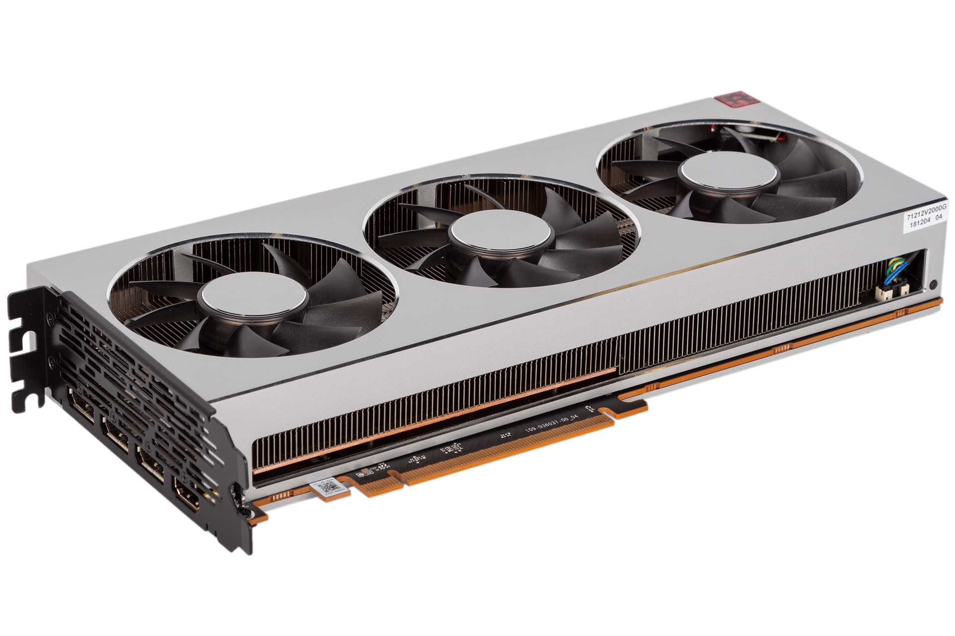
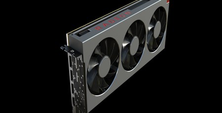
Now this GPU – Vega 20 – is making its gaming debut in the Radeon VII. Launching today for $700, since confirmed as £649 here in the UK, the Radeon VII is positioning itself against the RTX 2080, leaving RTX 2080 Ti comfortably ahead just as Vega 64 did with GTX 1080 Ti.
| AMD Radeon VII | AMD Radeon RX Vega 64 | AMD Radeon RX Vega 56 | |
| Architecture | GCN 5.1 | GCN 5th Gen | GCN 5th Gen |
| Codename | Vega 20 | Vega 10 | Vega 10 |
| Base Clock | 1,400MHz | 1,274MHz | 1,156MHz |
| Boost Clock | 1,750MHz | 1,546MHz | 1,471MHz |
| Peak Clock | 1,800MHz | 1,630MHz | 1,590MHz |
| Stream Processors | 3,840 | 4,096 | 3,584 |
| Compute Units | 60 NCUs | 64 NCUs | 56 NCUs |
| Texture Units | 240 | 256 | 224 |
| ROPs | 64 | 64 | 64 |
| Transistors | 13.2 billion | 12.5 billion | 12.5 billion |
| Die Size | 331mm2 | 495mm2 | 486mm2 |
| Process Node | 7nm | 14nm | 14nm |
| Memory | 16GB HBM2 | 8GB HBM2 | 8GB HBM2 |
| Memory Frequency | 1GHz (2Gbps effective) | 945MHz (1.89Gbps effective) | 800MHz (1.6Gbps effective) |
| Memory Interface | 4,096-bit | 2,048-bit | 2,048-bit |
| Memory Bandwidth | 1TB/s | 483.8GB/s | 409.6GB/s |
| Power Connectors | 2 x eight-pin | 2 x eight-pin | 2 x eight-pin |
| Stock Card Length | 267mm | 267mm | 267mm |
| Board Power | 300W | 295W | 210W |
If you need a refresher on Vega’s architecture you can head here. For the most part this is a die shrink, so the high level core layout hasn’t changed. As such the Vega 20 GPU has 64 Compute Units on-die, but in Radeon VII only 60 are enabled, leaving us with 3,840 cores and 240 texture units. AMD can produce this GPU with all cores enabled, as that’s what the Radeon Instinct MI60 is, but the Radeon VII’s configuration means it is instead based on the second-tier Instinct MI50. The full ROP count of 64 is maintained, thankfully.
CrossFire support has been ditched, however – AMD hasn’t given a reason for this, other than saying that Radeon VII still supports multi-GPU in any DX12/Vulkan titles that enable it.
AMD targets a similar power envelope to Vega 64 at 300W, allowing it to push clock speeds higher at similar voltage levels thanks to the new smaller process node. The boost clock is the most relevant, defined as ‘the typical achievable frequency in common workloads’, and at 1,750MHz this is 13 percent up on Vega 64. Peak frequency is exactly that, the highest you’ll see in from performance bursts, while base clock is the minimum guaranteed. If you recall that Nvidia’s RTX 2080 Ti and RTX 2080 are rated at 250W and 215W respectively (10W higher for Founders Editions), it seems clear already that even the new process won’t allow AMD to match Nvidia on efficiency.
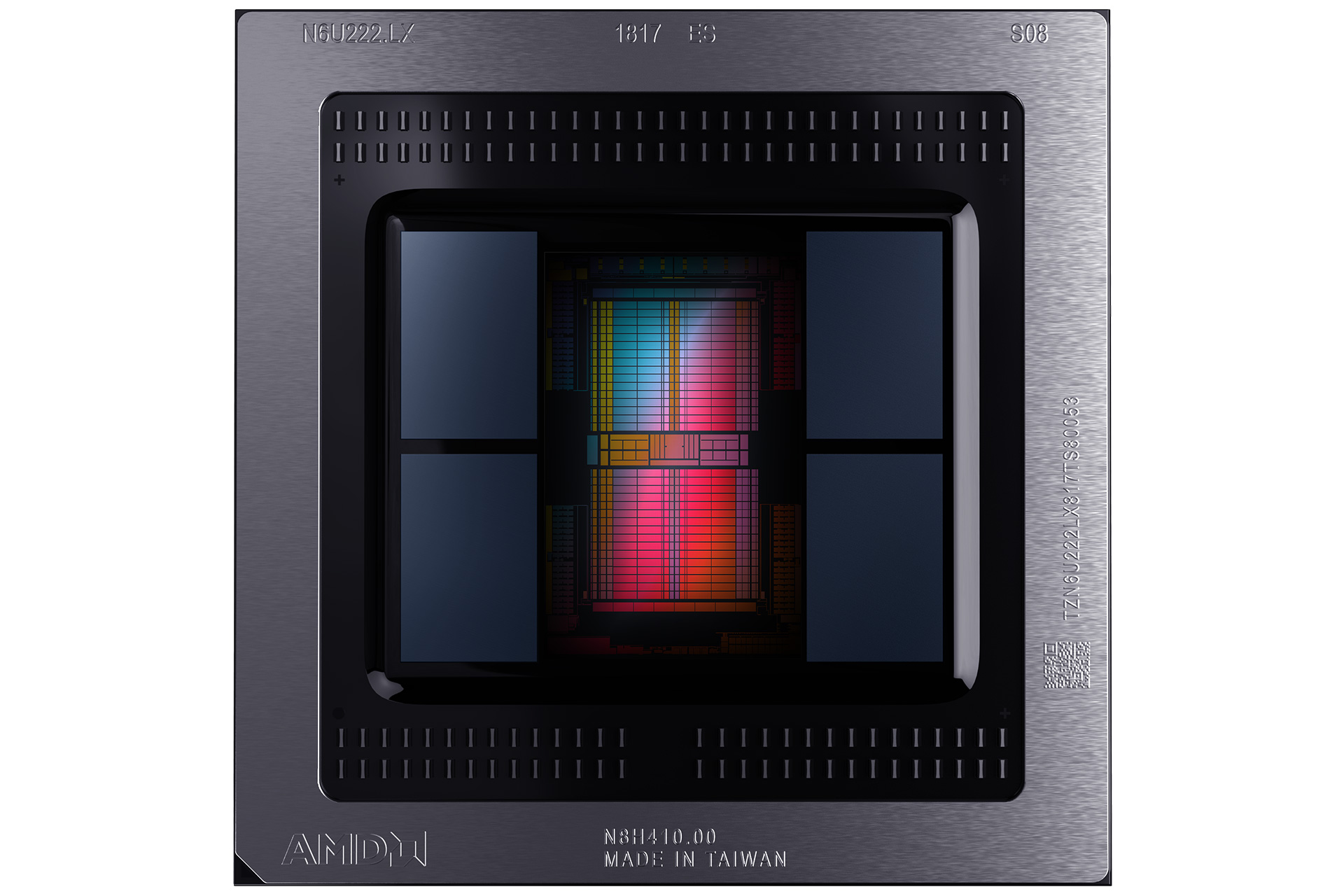
The biggest changes come on the memory side, and AMD is going all-out here. With a new die size of just 331mm2, there’s plenty of room on a similar size package for additional HBM2 memory, and AMD has taken full advantage by doubling the count from 8GB to 16GB, split evenly across four stacks. AMD’s Radeon Vega Frontier Edition also featured this amount of HBM2, but AMD has also widened the memory interface again by double compared to Vega 10 GPUs. Combined with a slightly higher memory clock speed, we get to a staggering 1TB/s of raw memory bandwidth, leaving Radeon VII with double the memory and more than double the available bandwidth of both Vega 64 and RTX 2080, and substantially more than even RTX 2080 Ti.
That’s impressive on paper, of course, but it does raise the question of whether or not it’s actually too much i.e. does a gaming GPU even at this level really need so much memory and bandwidth? AMD, of course, reckons it’s a benefit, both in professional/creative workflows (not a focus in our gaming GPU reviews) but also in games. Regarding the latter, AMD does offer some figures of how games at maximum settings are already going over 8GB of VRAM usage (take that, RTX 2080!), but such an analysis is potentially misleading, as using VRAM isn’t the same as needing it – only performance measurements can reveal actual bottlenecks. It’s also important to remember that compression algorithms can make up differences in memory bandwidth, so comparing AMD to Nvidia on this front isn’t quite as clear-cut as a glance at the figures.
While the core and memory configurations suggest Radeon VII is simply the Radeon Instinct MI50 in new clothes, then, there are some differences that come as a result of their different target markets. For example, the Radeon VII sticks to PCIe 3.0, as PCIe 4.0 is pointless for desktop consumers. Double-precision (FP64) performance is also capped at 1/4 the rate of single-precision (FP32) instead of 1/2, and the memory does not feature ECC.
You may see the Radeon VII referred to as having second-generation Vega architecture, but in the larger scheme it is still GCN 5th Gen, colloquially GCN 5.1. Optimisations include the already-mentioned wider memory interface, a selection of on-die latency/frequency boosts, increased ROP bandwidth, and additional floating point and integer accumulators to aid compute performance.
Finally, while traditional GPU monitoring software like GPU-Z report an easy-to-understand, single ‘GPU temperature’ reading, modern GPUs actually have multiple thermal sensors that are critical to successful and efficient dynamic performance control. For Radeon VII, AMD has doubled the sensor count to 64 and will be exposing to software a new measurement called ‘Junction Temperature’. Said to be a more accurate reflection of the GPU’s hottest parts, it also allows AMD to hit higher average boost clocks and deliver about two percent more performance when using it to manage performance instead of GPU temperature (AKA Edge Temperature).


MSI MPG Velox 100R Chassis Review
October 14 2021 | 15:04

Want to comment? Please log in.