Rock out with your ROP out
As well as the revised approach to stream processors, the new SMs also boast many more texture units. Whereas GF110’s 16 SMs each packed four texture units each (64 total) the eight SMs in GK104 boast 16 texture units each, doubling the total available texture units to 128. The number of load/store units and special function units per SM has also increased significantly to compensate for the truck load of extra stream processors.Despite the increased execution resources of each SM, there’s still only one PolyMorph Engine per SM, which, with the reduced SM count, means just eight in total; half that of GF110. The PolyMorph engine is the part of the GPU which acts as an intermediary throughout the rendering process, applying vertex fetch, tessellation, viewport transform, attribute setup, and stream output whilst passing the results to SMs in between each process. Once all stages are complete, the results are forwarded to the GPC’s rasteriser for final rendering. This reflects Nvidia’s more distributed approach to tessellation. Whereas AMD’s South Islands architecture handles tessellation in the front end engine, both Fermi and Kepler apply tessellation at an SM level.
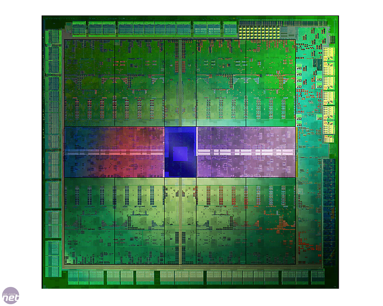
The Kepler architecture; it's a looker
Kepler’s memory subsystem and ROP layout has also been greatly altered in comparison to Fermi. GF110’s 384-bit memory interface (six 64-bit memory controllers) has been replaced with a 256-bit memory interface of four 64-bit memory controllers, each connected to 512MB of GDDR5 for a total of 2GB of VRAM. Impressively, Nvidia has managed to push this GDDR5 to exceedingly high frequencies, with the GTX 680 2GB’s memory running at 1.5GHz (6GHz effective). This means that despite the reduced memory interface, the resulting memory bandwidth is only a little slower than that of the GTX 580 1.5GB (192.26GB/sec vs. 192.4GB/sec), although this is still notably less than the 384-bit memory interface equipped HD 7970 3GB, capable of 264GB/sec.
More surprisingly though is Kepler’s ROP count, which has been reduced from the 48 ROPs of Fermi down to 32 (eight per memory controller). However, this reduction is somewhat counter-acted by Kepler’s increased core clock speed. Assuming the ROPs are unchanged between the two GPU architectures (which we’ve seen nothing to indicate otherwise) 32 Kepler ROPs (at 1,006MHz) are equivalent to 41 Fermi ROPs (at 772MHz). This is still a reduction, but it’s not as significant as it might first appear.
A word on scalability
Part of Fermi's eventual success in the guise of first the GTX 460 1GB and the GTX 580 1.5GB, 570 1.3GB and 560 Ti 1GB was its scalability. With 16 SMs to be switched off or tinkered with, we eventually saw three GPUs based on the GF110 GPU, running 512, 480 and 448 stream processors alongside varying core clock speeds. With Kepler’s larger SMs, disabling one is going to have a greater impact on performance. While we’re sure we’ll see lesser GPUs based around the Kepler architecture populating Nvidia’s range shortly, it’s unclear whether these will take the shape of similarly clocked versions with fewer SMs, or a revised design as with Fermi’s GF114 GPU, as used in the GTX 560 Ti 1GB.RELATED ARTICLES


MSI MPG Velox 100R Chassis Review
October 14 2021 | 15:04

Want to comment? Please log in.