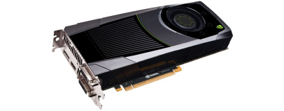
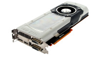
Keeping up with Kepler
The switch to the new 28nm production process has brought with it a new GPU architecture, replacing the 40nm Fermi GPU of the GTX 480 1.5GB (GF100) and GTX 580 1.5GB (GF110). Dubbed Kepler, this new 28nm architecture is neither a complete re-design nor a minor upgrade, keeping the basic layout of Fermi but with some significant alterations to the streaming multiprocessor (SM) design. The GPU at the heart of the GTX 680 2GB, dubbed GK104, represents the peak of the Kepler architecture, with the maximum amount of GPU assets. There’s no repeat of the GTX 480 1.5GB’s disabled SM here.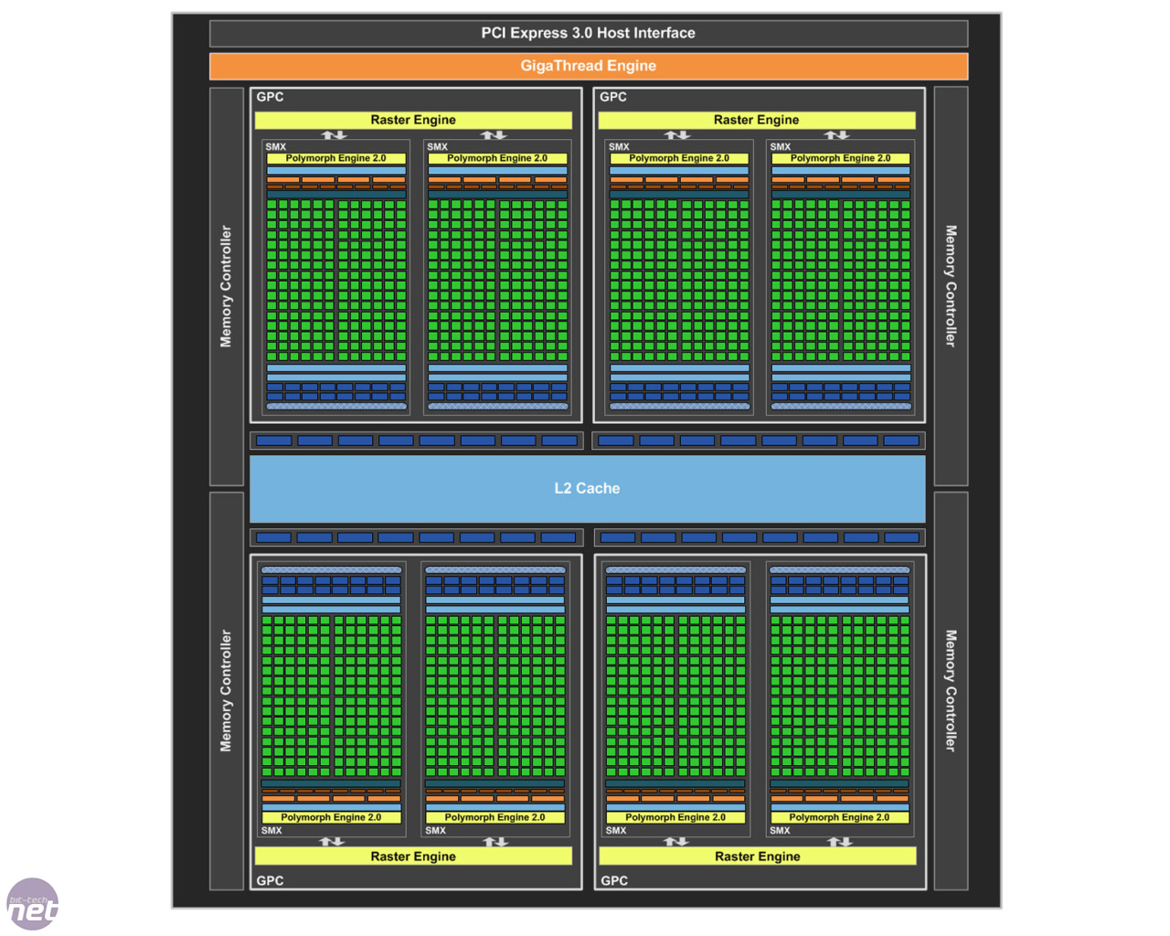
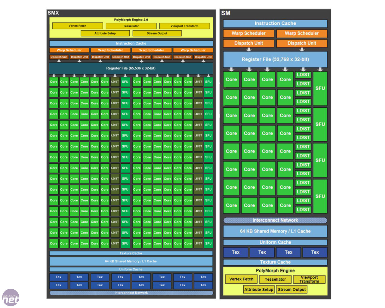
Click to enlarge - The Kepler Architecture and a side-by-side comparison of Kepler's SMX and Fermi's SM
As with Fermi, the GPU is split into four separate graphics processor clusters (GPCs), but each is now comprised of just a pair of SMs rather than four SMs apiece, in a similar fashion to the GTX 560 Ti 1GB's GF114 GPU. Each GPC still contains its own raster engine, but it’s within the SM that the real changes have been made. The new SMs, dubbed SMX (presumably Nvidia is competing with AMD’s ‘GCN’ for silliest GPU lingo 2012) have been completely redesigned, and now boast a whopping 192 stream processors each, as opposed to the 32 stream processors found in each SM with Fermi.
This huge increase in stream processor count to 1,536 for the whole GPU (tripled in comparison to the GTX 580 1.5GB’s 512 stream processors) has required some extra additions to each SM. The number of Warp Schedulers (the part that assigns render threads from the Gigathread engine to individual SMs) has doubled to four per SM (although the total number on the GPU remains 32) and each is now able to dispatch two instructions per clock thanks to a pair of instruction dispatch units for every Warp Scheduler.
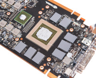
Click to enlarge
This doubles the GPU’s instruction per clock rate in comparison to Fermi, necessary when there are so many more stream processors to address. The scheduling functions themselves have also been redesigned and greatly simplified with a greater focus on power efficiency.
With so many more stream processors than its predecessor and an otherwise similar GPU layout, you’d be forgiven for expecting a quite extraordinary threefold increase in performance. Sadly, that’s not quite the case, as Nvidia has chosen to scrap the separate shader clock, long a defining feature of its GPUs.
This means the whole GPU, stream processors and all, runs at a nippy base clock of 1,006MHz. This is the same way that AMD’s GPUs have operated for years and is another example of the two companies moving in the same direction when it comes to GPU design. The loss of the higher shader clock (presumably due to the power and heat constraints of so many stream processors) means that, in comparison to the GTX 580 1.5GB, each stream processor is actually running 5,44MHz (35 per cent) slower, although there are now three times as many of them.
RELATED ARTICLES


MSI MPG Velox 100R Chassis Review
October 14 2021 | 15:04

Want to comment? Please log in.