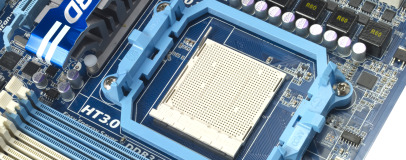
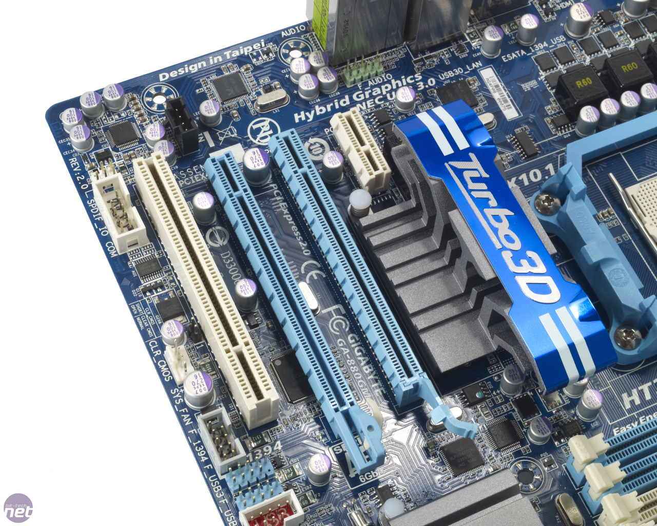
GA-880GMA-UD2H Layout
As it’s based on the m-ATX form factor, the UD2H can look a little cluttered at times. This is pretty much par for the course with smaller boards, but Gigabyte has made a number of design choices that exacerbate the problem.The most glaring flaw is the positioning of the five SATA 6Gbps ports (the sixth port of the SB850 Southbridge is tasked with eSATA duties) as these lie directly in line with where a long dual-slot graphics card will sit. With our standard Radeon HD 5870 installed only two of the SATA ports were usable; we couldn’t even fit right-angled SATA connectors into the sockets without them fouling the graphics card. Admittedly this isn’t going to be a problem for anyone with a smaller graphics card (you’ve got 205mm before you start covering the ports, if you’re interested) but it’s still a glaring error, especially when SATA 6Gbps is one of the headline features of the board.
Click to enlarge
The 24-pin ATX power connector is at least located on the edge of the board, which will help cable routeing; the IDE and floppy ports on the other hand are a little more inland. Frustratingly, the location of the IDE and floppy port connectors push the DDR3 slots very close to the CPU socket, which means you could have problems fitting a large CPU cooler and memory with tall heatsinks.
The centre of the board is dominated by a smart heatsink that sits astride the 880G chipset. This sits extremely close to the PCI-E 1x slot and while none of the cards we tried in this slot actually clashed with the heatsink, it could still be a problem if you have a card with an oversized EMI shield or heatsink. We also found both the 880G heatsink and the Southbridge heatsink to be poorly mounted: both wobbled freely with a minimum of force.
GA-880GMA-UD2H Overclocking
Despite the fact that the UD2H is most likely to find its home in HTPCs or budget builds, we still wanted to put it through the overclocking mill at least once to see what it was made of. Things started well for the board, as we were pleasantly surprised by the amount of options on show in the Motherboard Intelligent Tweaker section of the BIOS.
Click to enlarge
First off we wanted to find the board's highest HTT clock. For this we lowered the multiplier down to 10x or so, added extra voltage and steadily increased the HTT clock until the board flaked out. The UD2H achieved a passable maximum HTT of 330MHz, which is only 20MHz or so below the highest frequency we've seen - a commendable effort for a budget board.
We then turned our attention to the overclocking proper - overclocking AMD's Phenom X3 720 BE to its air cooled maximum of 3.7GHz. We’re happy to report that the UD2H could, though we had to use a slightly lower HTT clock and higher multiplier than with other boards. We eventually settled on a HTT clock of 308MHz and a multiplier of 12x which gave an overall frequency of 3.69GHz. To achieve this we raised the CPU vcore from 1.325V to 1.5V, the Northbridge voltage from 1.2V to 1.3V and the confusingly titled NB/PCIe/PLL voltage from 1.8V to 1.9V.
We also had a quick play with Gigabyte’s Auto Unlock feature which managed to find and unlock the fourth core of our CPU. This was as simple as changing a setting in the BIOS, but still isn’t as convenient the Asus method of using an on-board button to perform the same function.


MSI MPG Velox 100R Chassis Review
October 14 2021 | 15:04

Want to comment? Please log in.