
Read and Write Levelling
The Read-Write Levelling feature is built into DDR3 memory controller to compensate for these Clock Skew issues.Boehm explains the problem with the new topology, “The clocks, commands, and addresses, are all routed to each DRAM in a ‘Fly-by’ and the DQ [Data] bus which includes the strobes is routed more like what the T-Branch was. The time that the commands, addresses and clocks arrive at each DRAM is a bit different, while the DQ signals arrive at roughly the same time. So you have this inherent skew between the DQ bus and the Clock at each DRAM with Fly-by, which causes problems that you have to resolve by de-skewing [at the other end] to get everything lined up again.
“That is where Write Levelling in DDR3 comes in. What you’re doing is you’re delaying the DQ bus slightly so that it arrives at each DRAM the same time the Clock does.” The memory controller dynamically aligns the Data-Data Strobes (DQ-DQS) to the Clock (CK) for each DRAM chip.
This is done with a simple ‘Hello-and-Respond’ feedback analysis. Once the amount of delay or skew to each DRAM chip is determined, the memory controller can easily compensate for the problem for subsequent activities.
DDR3 uses a new Multi-Purpose Register (MPR) for the signal Levelling process; this generates a pre-determined data pattern for calibration purposes during initialisation. The MPR helps the memory controller calibration by dynamically adjusting the data strobes as close to the centre of the Data Eye as possible.
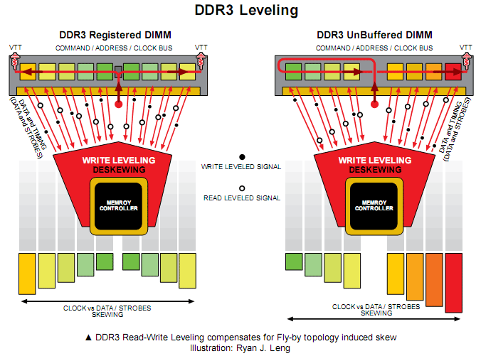
When the memory controller is in Write Levelling mode, at least one data bit must carry the levelling feedback to the memory controller across the DRAM configurations of x4, x8 or x16. After finishing calibration, a Write Levelling disabling sequence will be initiated by the memory controller.
The Levelling process happens from the other way as well; Read Levelling, as the name implies, aligns the Data bus to the Command-Address-Clock bus for the read cycle. After the memory controller Levelling calibration procedures, the memory comes back into standard operational mode.
An Analogy: Multiple Airport Pickups
Imagine you have to pick up eight relatives flying in for a holiday reunion. Each person arrives at a different time.Initially you don’t have everyone’s schedule, so you have to call everyone before they leave their respective homes. The act of calling everyone to confirm their arrival is what the Multi-Purpose Register (MPR) does within Memory Controller.
Once you know when everyone will arrive, you will arrange individual pickup times, with the earliest first and the latest last. You are the Data (DQ), your car is the Data Strobe (DQS), the airport is the Memory Module and the relatives are the Command-Address-Clock signals that fly in via the Fly-by path. Each person will arrive at a different gate, representing the DRAM Chip.
RELATED ARTICLES


MSI MPG Velox 100R Chassis Review
October 14 2021 | 15:04

Want to comment? Please log in.