
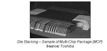
Stacking Technology and Increasing Capacity
Stacking methods are commonly used to economically increase the density of PC memory, by adding additional layers – dies, ICs and/or PCBs. These are commonly classified under two types of arrangements: Card-on-Card and Package-on-Package.To increase single chip density, Multi-Chip Package (MCP) stacking technology is used with BGA chips. Instead of having multiple chips lined along a DIMM side, each die is stacked on top of each other within a single Chip package. DRAM manufacturers may have their own proprietary wafer thinning and miniaturisation technologies to achieve smaller packaging and higher die count.
As of 2007 onwards, Samsung Semiconductors is expected to use its proprietary “Through Silicon Via” (TSV) with an all-DRAM stacking configuration – this design is neater, smaller, faster and consumes less power. However, Samsung is not the only one to use this technology, Intel has also previously demonstrated it back at IDF last Spring with its demonstration of Terascale technology, where it stacked memory on top of an 80 core processor.
The problem with today’s MCP technique is that different layers of DRAM are connected by fragile wire bonding. This configuration requires vertical gaps between layers that are tens of microns deep and these kinds of connections also require horizontal spacing on the package board hundreds of microns wide for the die-connecting wires. This kind of technological precision is expensive and very difficult to quality control, as a single wire short in hundreds is difficult to find and even more difficult to correct.
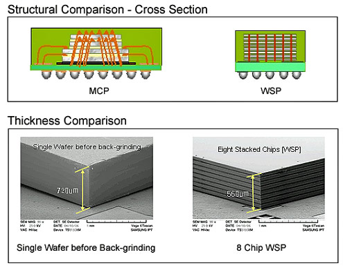
Samsung Wafer-level-processed Stacked Package
Source: Samsung Electronics
According to Samsung, its Wafer-level-processed Stacked Package (WSP) technology “forms laser-cut micron-sized holes that penetrate the silicon vertically to connect the memory circuits directly with a copper (Cu) filling, eliminating the need for gaps of extra space and wires protruding beyond the sides of the dies. These advantages permit Samsung’s WSP to offer a significantly smaller footprint and thinner package.”
The latest result is an improved 4GB DDR2 memory module from Samsung with better performance characteristics. Each chip will consist of four layers of 512 Megabit DRAM, giving it a two Gigabit per chip density. The upgraded TSV technique is expected to be used in DDR3.
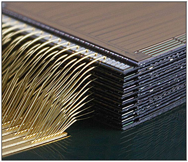
The World’s thinnest 1.4mm MCP with 20 Stacked Dies
Source: Elpida Memory
Akita Elpida Memory, in first half of 2007 successfully developed a 1.4mm high MCP with an amazing 20 dies stacked inside. A unique grinding technique is used to achieve 30µm thick chips and additional innovations were made in handling these tiny chips, wire bonding and resin injection into the narrow gaps to electrically insulate the layers from each other. To top things off, it is expected to be high-yield and low-cost – it is quite frankly, an amazing achievement.
RELATED ARTICLES


MSI MPG Velox 100R Chassis Review
October 14 2021 | 15:04

Want to comment? Please log in.