An Overview of High-Bandwidth Memory (HBM)
As previously outlined, bandwidth per watt and bandwidth per mm2 are the two main challenges facing GDDR5, and HBM addresses both. The new design is more than three times as efficient, delivering higher bandwidth at significantly lower power. This rebalances the ratio of DRAM and processor power consumption for future scaling and makes more power available to the GPU in graphics solutions, meaning performance can continue to scale upwards.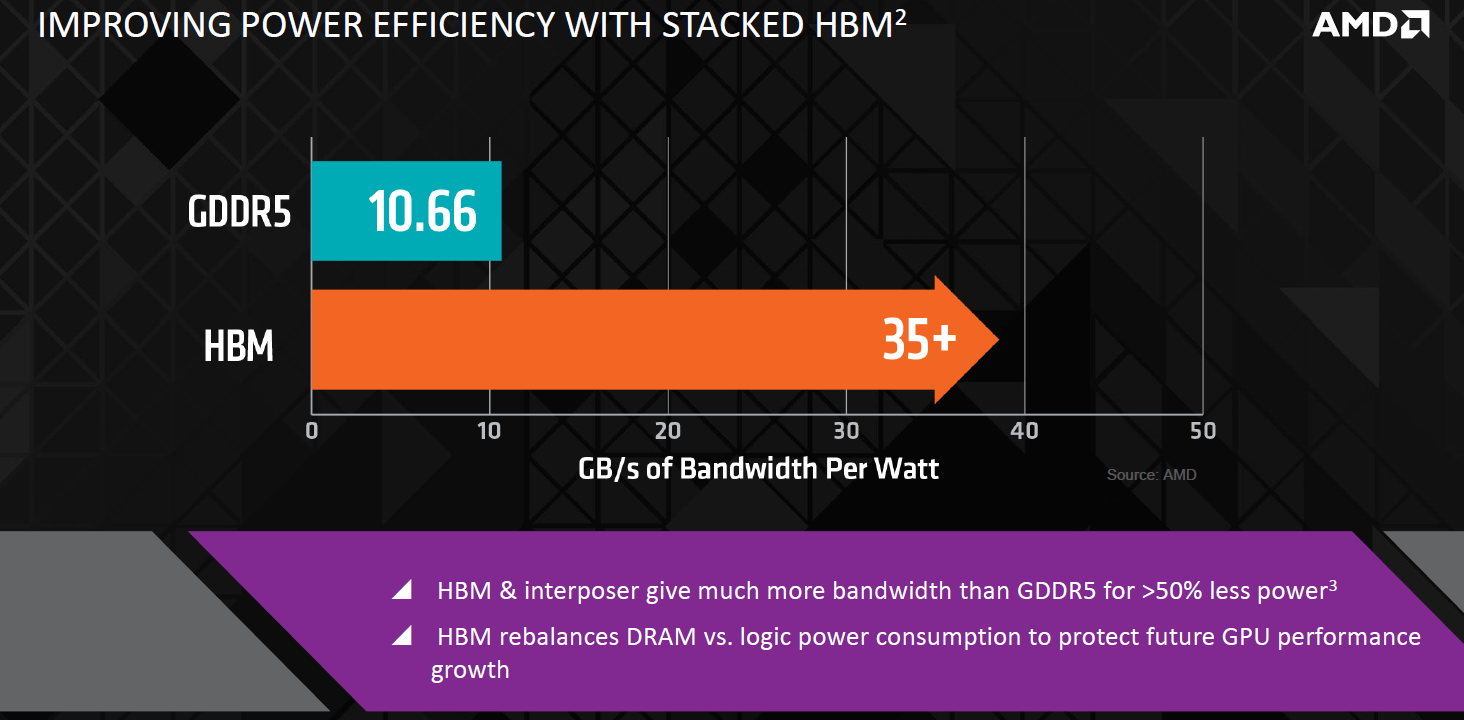
Click to enlarge
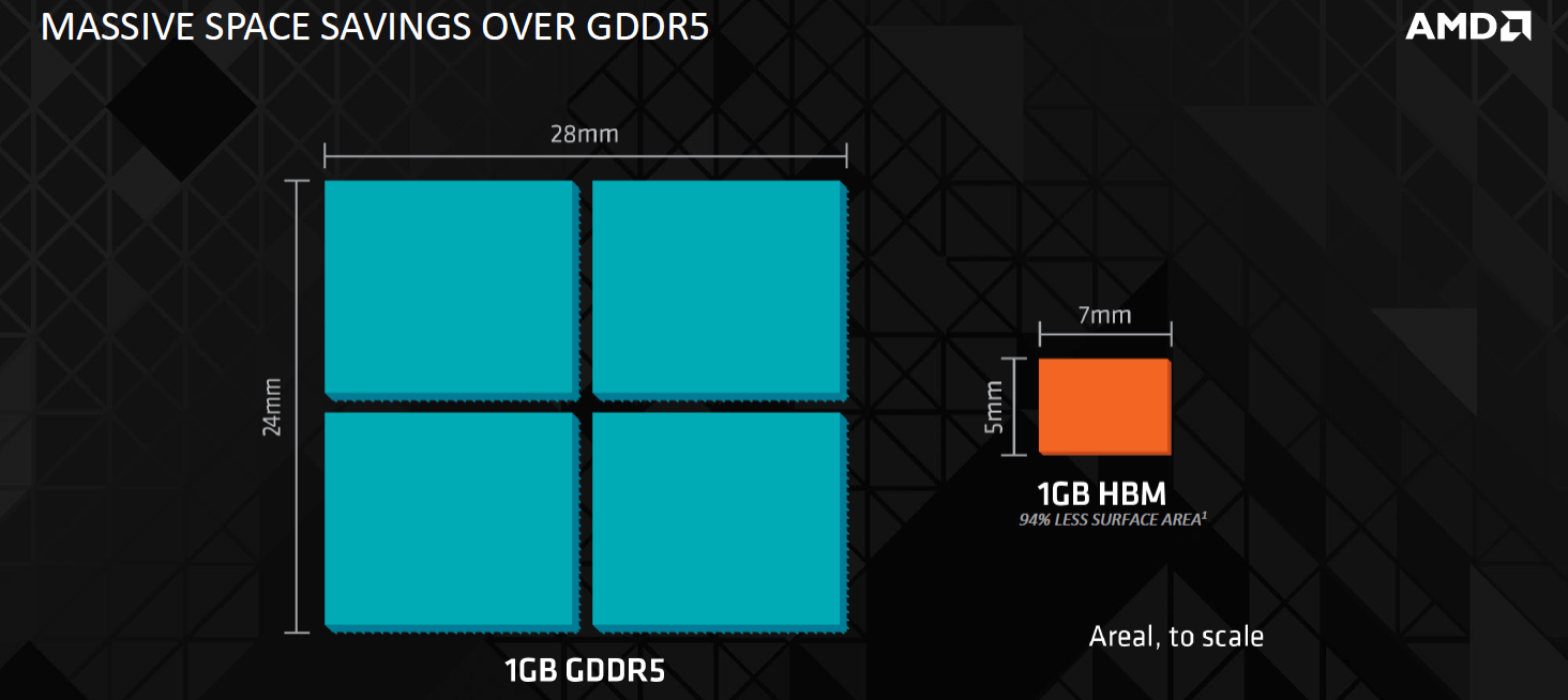
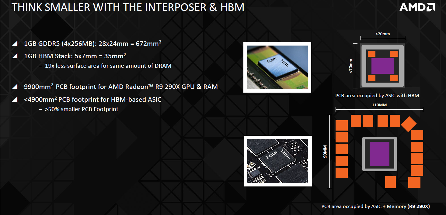
The space savings outlined by AMD below are a little inflated, since the 1GB of GDDR5 they show uses four 2Gb GDDR5 dies. While these are the most common, 4Gb ones are readily available and used in current graphics solutions, and with 8Gb ones now also being produced by Samsung, you only need one to reach 1GB. That said, the 1GB HBM stack is still significantly smaller and its bandwidth is four times higher than a single 8Gb GDDR5 chip. When using four 2Gb chips as shown, the HBM bandwidth is only a little higher, but then the space savings really are massive. The benefits of this will mainly be felt when HBM is adopted into smaller and mobile form factors.
Click to enlarge
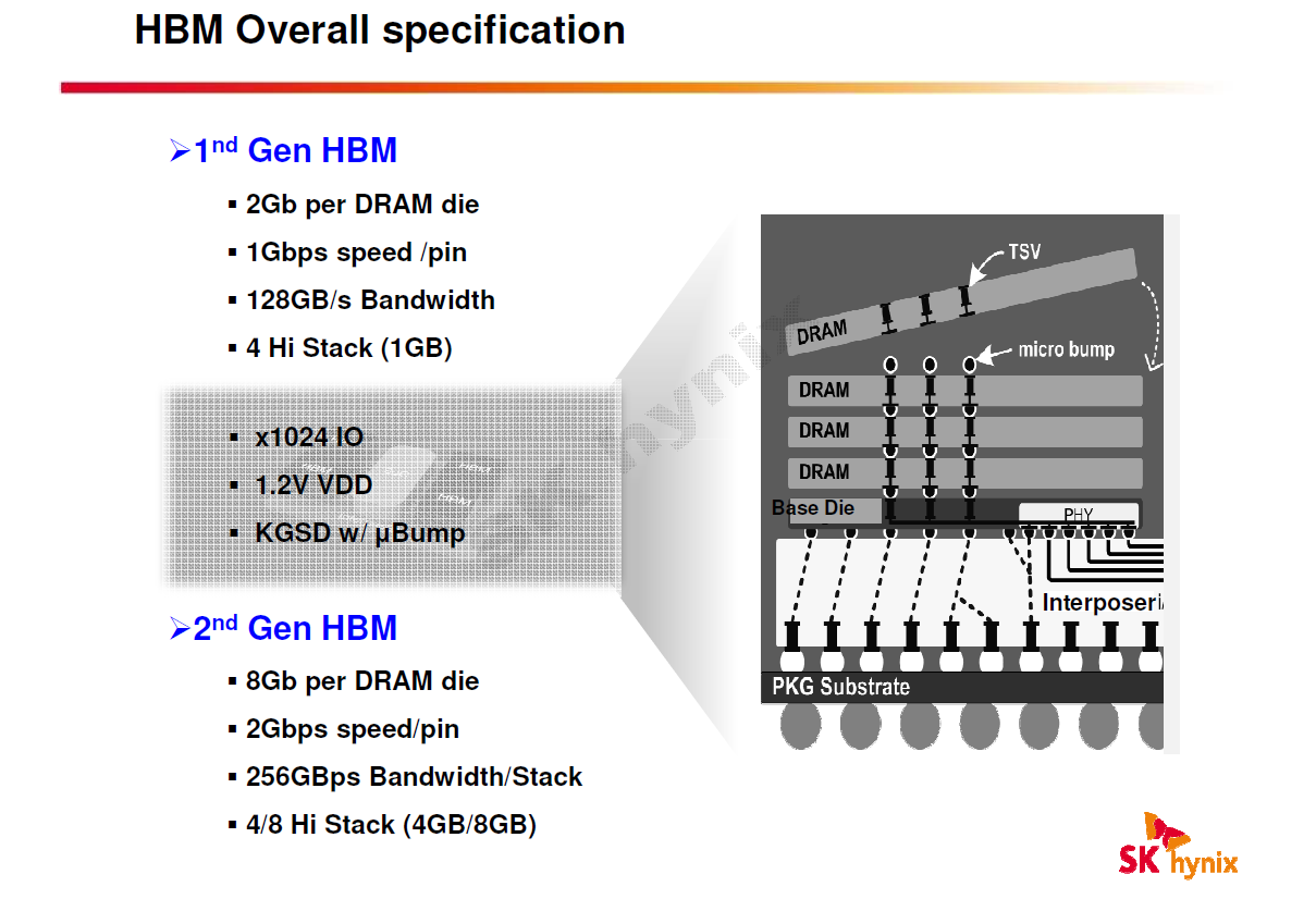
The implementation of HBM we've been discussing so far is only the first generation, which is capable of achieving 1GB in a single stack of four 2Gb dies with a 1GHz effective clock for 128GB/sec of bandwidth per stack. However, SK Hynix has already outlined separately what to expect from the second generation – each die will have an 8Gb capacity (whether 4Gb will be skipped or not we don't know), and stacks will have either four or eight dies in total (4GB or 8GB per stack). Effective clocks will reach 2GHz, meaning 256GB/sec per stack. AMD even said that 16-high stacks might be possible in the future, although that's obviously some way off.
Click to enlarge
Back to the here and now, there have been rumours flying around recently that AMD's next generation of GPUs will be limited to 4GB frame buffers when using HBM, and we can confirm this is the case. While AMD is still only referring to a 'HBM-based ASIC', the designs all show a GPU flanked by four HBM stacks, which as we know are currently limited to 1GB each. We're not clear on the reason for the four stack limit (possibly memory controller design), but AMD insists that 4GB is not going to be a limitation, even at high resolutions. Joe Macri, CTO Client & Graphics, AMD, claimed that 'you'd be blown away at how much [frame buffer] is wasted' and AMD has invested in making better use of the frame buffer, although the company didn't go into specifics. The additional potential bandwidth will help too, and it's worth noting that Nvidia's next generation of GPUs, Pascal, will use HBM as well, and so the green team may face similar limits – the latest available Pascal renders certainly suggest a four stack solution.
Click to enlarge
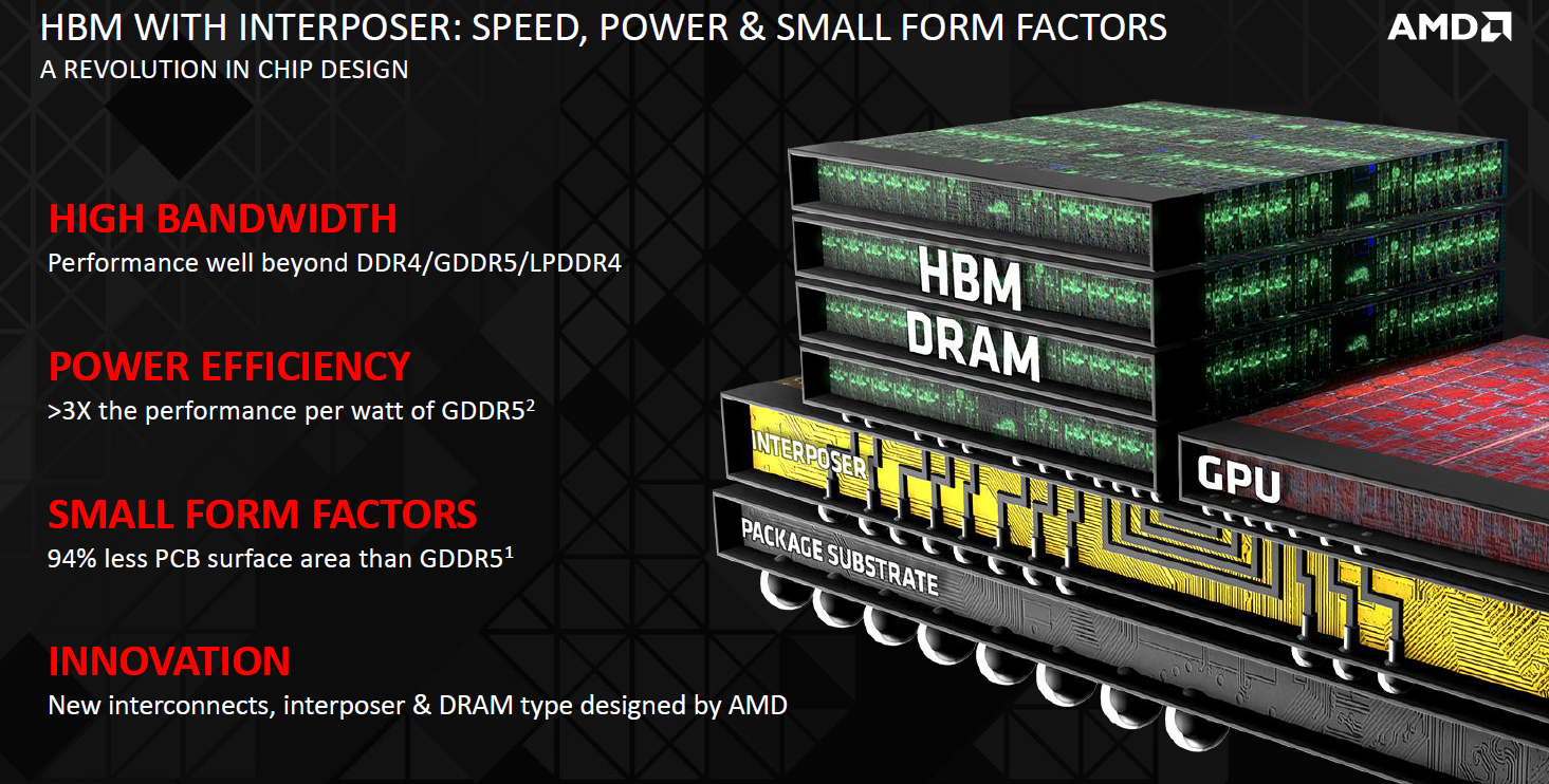
The new design is referred to as a 2.5D package as it has some vertical stacking but isn't a truly 3D package with DRAM atop GPU. This has some interesting implications for cooling. Physically, the DRAM stacks and GPU are at approximately the same height, but the package will be topped by a flat heatspreader with thermal contact material between it, the memory and the GPU. In this way, AMD says, the high-bandwidth memory acts as a heatsink for the GPU, adding surface area to the overall solution – cooling was actually less of a challenge than they originally thought. Still, if the TDP of the new cards is in line with the R9 290-series, let's hope AMD has developed a superior reference cooler or has third-party models ready on day one.
With the R9 300 series still pegged for a Q2 2015 launch, it shouldn't be long now before the first HBM-enabled devices reach the market. While the technology will launch initially at the high-end, where it's needed most for performance but where high volumes aren't as critical, it will clearly benefit lower-end devices in the future too. In particular, it's easy to see AMD's APUs eventually migrating to HBM, as they are very memory bandwidth limited in graphics processing tasks – in fact, AMD all but confirmed this would happen.
Click to enlarge
With other manufacturers besides Hynix also set to start HBM production and Nvidia already confirmed to be using it with Pascal, it's clear the technology is going to become evermore commonplace in many fields – the space and power savings will be critical to developments in mobile devices, while the higher bandwidth and future scaling will be seen favourably by high performance compute manufacturers. Memory can be a tough topic to get excited about, but we're certainly keen to see what the red and green teams can do with HBM-enabled GPUs.


MSI MPG Velox 100R Chassis Review
October 14 2021 | 15:04

Want to comment? Please log in.