
R600 Overview:
When ATI started designing the R600 architecture in 2003, the architects looked at its previous designs and picked through the best ideas from each of them. If you’re familiar with the R520 and R580 architectures, you’ll see that there are some familiar features in the new architecture.It’s also quite clear that R600 is the next progression on from the Xenos architecture (as featured in Xbox 360). R600 takes many of the ideas from that chip and refines them so that the design is better suited for PC graphics. If we jog our memory back to our interview with ATI’s Richard Huddy, he stated that he’d be “very surprised” if the 10MB Embedded DRAM module (the second die on the Xenos chip package, which is responsible for blending and outputting the pixels onto the screen) made an appearance on the PC any time soon.
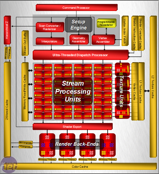
Another example of this is that the Xenos chip has 48 shader ALUs that can each co-issue a Vec4 and a Scalar instruction simultaneously every clock cycle. The Vec4 unit is quite specialised, and the next logical step was to move to a completely scalar architecture. This is where R600 takes this a step further as Xenos’ shader ALUs have been replaced with superscalar shader units that can co-issue up to five FP MAD (multiply-add) instructions or a single vector instruction per clock.
AMD's R600 graphics processing unit – flow diagram
There are also more of the shader units, too – R600 features 64 five-way superscalar shader processors, making a total of 320 stream processors. These are split into four shader clusters each with 80 stream processors or 16 shader processors (taking into account five stream processors per shader processor). The shader processors support FP32 precision for all mathematical operations. AMD’s R600 architecture is a superscalar VLIW (very large instruction word) design that can issue up to six independent instructions (five mathematical and one flow control) in each superscalar shader processor.
R600 also features 16 texture mapping units (TMUs), 16 ROPs (or render backends, as AMD refers to them) and the world’s first external 512-bit memory interface that helps the Radeon HD 2900 XT break through the 100GB/sec memory bandwidth barrier with relative ease. Of course, the first graphics card to break through the 100GB/sec barrier was actually Nvidia’s GeForce 8800 Ultra, but that card retails at almost double the price of the HD 2900 XT.
In addition to this, probably the most exciting portion of R600 is actually the programmable tessellation unit, which is very similar to the one inside the Xbox 360’s Xenos chip. This feature goes beyond the DirectX 10 specifications and it’s unclear when Microsoft plans to introduce this into its API. When we spoke with Microsoft’s David Blythe at Nvidia's G80 launch, he said that tessellation was a feature that the DirectX architects definitely wanted to include in a future version of DirectX, but he couldn’t give us a definite time frame.
Let’s dive a bit deeper...
RELATED ARTICLES


MSI MPG Velox 100R Chassis Review
October 14 2021 | 15:04

Want to comment? Please log in.