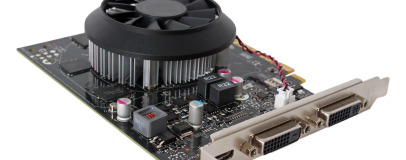
First Generation Maxwell Architecture
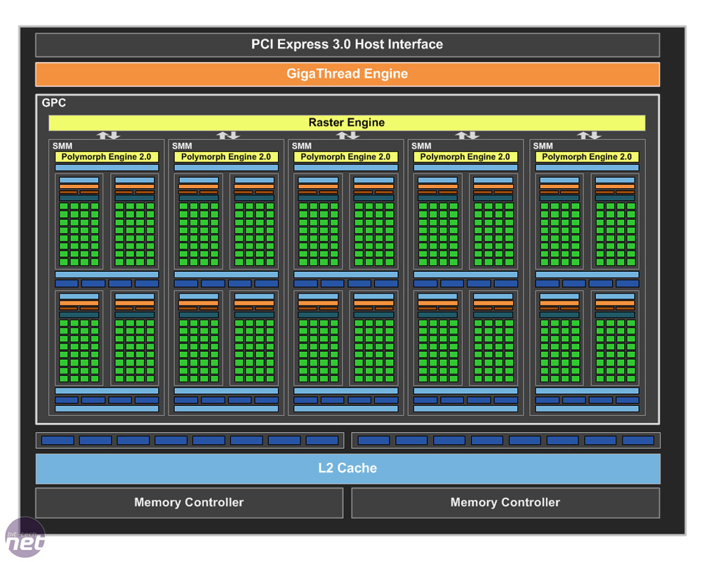
Nvidia claims that it has been able to achieve a doubling of performance per watt with Maxwell compared to Kepler. This is impressive if true, as Maxwell is made on the exact same TSMC 28nm process (perhaps 'second generation' Maxwell processors will be 20nm, though this is pure speculation). As you'd expect, Nvidia has made numerous microarchitectural tweaks and improvements to achieve this, and has tuned Maxwell down to the transistor level. The first new chip with these tweaks, which is fully enabled in the GTX 750 Ti, is called GM107. It's a 1.87 billion transistor chip with a 148mm2 die size.At a high level, there are many similarities between Maxwell and Kepler. The new architecture still comprises graphics processing clusters (GPCs) that feature a single raster engine each. The GPCs are subdivided into streaming multiprocessors (SMMs, previously SMXs) which themselves house a Polymorph engine (featuring a single tesselator) and numerous CUDA cores. Meanwhile, ROPs are again aligned with L2 cache segments and memory controllers.
Click to enlarge
However, the SM, which is the main building block of an Nvidia GPU, has been redesigned, and it's this that is the main driver of the improved efficiency. With Kepler, an SMX was a single block of 192 CUDA cores, with some of these shared between parts of the scheduling and dispatch hardware. Maxwell's SMMs, however, are divided into four separate processing blocks of 32 cores each (128 overall), and each block is equipped with its own instruction buffer, scheduler and dispatch units. Partitioning the cores into smaller, power-of-two blocks like this makes scheduling simpler and increases parallelism. Along with offloading certain scheduling duties to its compiler software, this has allowed Nvidia to tweak the scheduling hardware and algorithms to be smaller, less power hungry and faster.
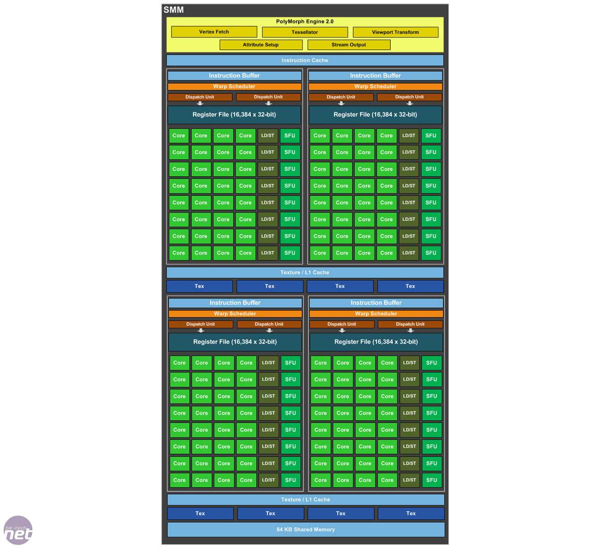
Click to enlarge - the redesigned Maxwell SM
As a result of this more efficient scheduling, there are fewer unnecessary stalls within the pipeline and a higher count of instructions issued per cycle. Along with the simpler and more parallel core layout, it also allows for improved workload balancing and grants Maxwell greater overall utilisation of the cores, with more of them working together at once and less of them doing nothing other than drawing power.
These changes to the SM mean that the new design can deliver about 35 percent more performance per core in shader limited workloads and, overall, about 90 percent of the performance of a Kepler SM despite having a third less CUDA cores and occupying a significantly smaller area.
Elsewhere within the SM, each pair of processing blocks shares four texture units (meaning there are now eight rather than sixteen per SM) and a texture cache. All four blocks also have access to a separate 64KB of shared memory, but compute L1 cache functionality has been moved out of this and into the texture cache.
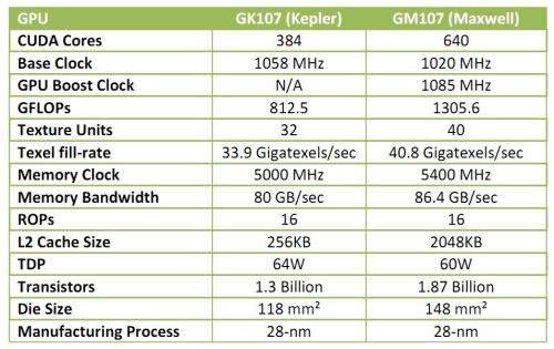
Maxwell also brings with it a massive increase to L2 cache size. Even in the small GM107 chip, it's 2MB in size, which is eight times larger than the 256KB one of GK107 (the GTX 650's GPU) and 512KB more than the mighty GK110 in the GTX 780 Ti. This translates into less calls to the main GPU memory, which consumes more power and is higher latency. Nvidia also cites improvements to internal memory bandwidth and efficiency.
Other efficiency tweaks include making the onboard H.264 hardware video encoder and decoder (NVENC) faster for both operations, and equipping it with a local decode cache for more efficient decoding. Finally, the GC5 low power sleep state is introduced, specifically for light workloads such as a video playback, which is likely to be more beneficial in the mobile market.
Taking GM107 as a whole, we see that its single GPC houses five SMs (it thus has one rasteriser and five tesselators). With Kepler, we only ever saw a maximum of three SMs per GPC – Maxwell's space saving SM design means Nvidia can implement more per GPU. The five SMs mean GM107 has a total of 640 CUDA cores and 40 texture units. It also has 16 ROPs and two 64-bit memory controllers.
The GTX 750 Ti's base GPU clock speed is 1,020MHz, but as it features GPU Boost 2.0 it will boost past this in use. The typical boost clock is listed as 1,085MHz, but our sample happily boosted to a constant 1,150MHz. This is fairly high as GPUs go, but Nvidia also claims that the card is massively overclockable – we'll certainly be putting this to the test.
As for memory, the GTX 750 Ti will be available in 1GB and 2GB flavours, with 2GB being the reference specification and the most common among board partners (as well as the one we're reviewing). Its GDDR5 is clocked by default at 1.35GHz (5.4GHz effective). Therefore, while its 128-bit memory interface is the same as GK107's, it has a slightly increased total memory bandwidth of 86.4GB/sec. The much larger L2 cache will also help to reduce memory bandwidth as a bottleneck.
The specifications certainly suggest that efficiency has been much improved. When comparing GM107 to the older GK107, we see that for a modest 25 percent die size increase you get a 67 percent increase in CUDA cores and 44 percent more transistors. Clock speeds are also higher (with Boost), but the new card is within the same power envelope as the GTX 650 and forgoes the need for an external power connection too.
RELATED ARTICLES


MSI MPG Velox 100R Chassis Review
October 14 2021 | 15:04

Want to comment? Please log in.