
GT200 compute architecture
For those of you that are familiar with G80’s scalable processor array architecture, you should find it fairly easy to get to grips with what’s behind the GeForce GTX 200-series GPUs.GT200 also uses a scalable processor array design, but some areas of the GPU have been re-engineered, while other areas have been suitably beefed up to better-cope with today’s (and tomorrow’s) 3D graphics and massively parallel processing tasks.
You see, Nvidia’s GPUs are no longer just about their 3D graphics capabilities because, with the introduction of CUDA and a slew of GPU-accelerated general computing applications, there’s much more to think about these days. And, as a matter of fact, Nvidia introduced the GT200 GPU by first talking about its general compute capabilities.
There are no two ways about it – Nvidia’s GT200 GPU is an absolute brute. It’s manufactured using TSMC’s 65nm process, features approximately 1.4 billion transistors and packs a total of 240 thread processors running at 1,296MHz (on the GeForce GTX 280) – the result is a GPU that delivers 933.12 gigaFLOPS of compute power at peak. These numbers alone make it the largest and most complex GPU ever to be made.
Nvidia's GT200 GPU - compute flow diagram
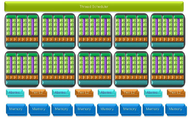
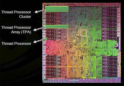
The 240 thread processors are split down into ten thread processing clusters (TPCs), with each broken down into three streaming multiprocessors (SMs) or thread processing arrays (TPAs). Threads are assigned by the thread scheduler, which talks directly to each streaming multiprocessor through a dedicated instruction unit; this then assigns tasks to one of eight thread (or stream) processors.
Each streaming multiprocessor also has its own 16KB of shared local memory – Nvidia said it included this in order to reduce external bandwidth usage as it enables the thread processors to communicate with one another directly (inside each SM) without having to leave the chip and it's also there to allow compute programs to access a local store with predictable latency. This shared local memory runs at the same clock speed as the thread processors.
Moving closer into the streaming multiprocessors, Nvidia says each thread processor inside the SM can now perform "near full speed dual-issue of multiply-add ops (MAD) and MULs." It achieves this by using two special function units (SFUs) in each SM to execute transcendental calculations, attribute interpolation and for performing floating point MUL instructions. So, in order to achieve this, you use the thread processor's MAD unit to perform a MUL and an ADD in the same clock, and then use the SFU to perform another MUL at the same time.
With this in mind, the units have 50 percent higher compute throughput per clock than a typical G8x thread processor (three FLOPS per clock on GT200, compared to two FLOPS per clock on G8x), meaning each GTX 280 thread processor can deliver 3.89 gigaFLOPS of single precision, IEEE 754, floating point performance. On the other hand, G80’s thread processors could only work on one MAD operation per clock in most situations, but there were a select few scenarios where you could dual-issue MAD and MUL ops.
In addition to this, the thread processors now feature support for double precision, but this requires a dedicated execution unit and these tasks run at one twelfth speed. The unit can handle one double precision MAD per clock (there's no dual-issue MAD+MUL), meaning the maximum throughput for the GPU when it's only processing double precision calculations is 77.76 GigaFLOPS.
What's more, you can only allocate single or double precision operations to each thread processing cluster – you can’t increase the granularity any further than this, meaning you can’t assign double precision ops to a single streaming multiprocessor.
Part of the reason for this is the eight texture units and local L1 texture cache inside each TPC. At this point, you’re probably wondering why I’ve mentioned texture units in the parallel computing side of GT200’s architecture – the reason is because they’re still used for various filtering operations when the GPU is running in compute mode. The texture units themselves run at a lower clock speed to the rest of the TPC – they actually run at 602MHz on the GeForce GTX 280 and this is defined by Nvidia as the ‘core’ clock.
Moving further down the compute pipeline, Nvidia also includes four ‘Atomic’ units – these are designed to handle certain atomic read-modify-write commands with direct access to the memory. These operations bypass the chip’s caches altogether and the atomic unit provides granular access to memory locations, facilitating parallel reductions and parallel data structure management.
I've asked Nvidia for more information on the atomic units' capabilities, including how many data exports per clock we can expect with 64-bit and 128-bit values and also what clock speed they run at, but until now the company has been reluctant to provide any more detail.
RELATED ARTICLES


MSI MPG Velox 100R Chassis Review
October 14 2021 | 15:04

Want to comment? Please log in.