
We have heard many rumours floating about the web regarding the specifications of G70, and our own initial estimates were fairly close. G70 is based on TSMC's 0.11-micron manufacturing process, as has already been used by NV41, NV42, NV43 and NV44. We're not too sure why NVIDIA have chosen to re-label their GPU's code names, there is any number of reasons why they might have done this. We believe it is because NVIDIA's business is not solely based around the design of graphics processing units, as they're a reputable force in the chipset market too – with over 50% market share on AMD-based platforms. 'G' for graphics processor certainly makes sense, much like 'C' for chipset does.
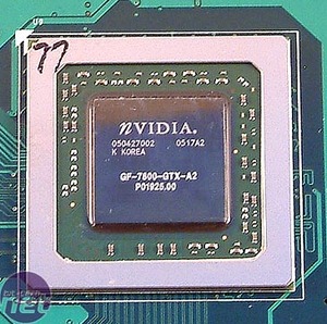
 Physically, the die is slightly bigger than NV40 was, but not by a great deal; in terms of transistor counts, G70 is massive in comparison. G70 contains 302 million transistors in comparison to the 220 million that were in NV40, making it over 35% larger than its elder sibling. That's a hell of a lot of transistors by any stretch of the imagination, especially when you take the fact that the Athlon 64 FX-55 only has 105.9 million transistors in to account – G70 is almost three times as complex as an FX-55.
Where do you spend those extra transistors when you consider that NV40 wasn't exactly a simple graphics-processing unit?
Well, NVIDIA have spent their time improving the efficiency of NV40, and in essence, G70 is from the same parent family as the original NV40, much like the GPU for the upcoming Sony Playstation 3 – they're all based on the same architecture, but NV40 was designed with expansion and efficiency in mind. If you remember back to April last year, the diagram below will ring a bell or two – the flow diagram follows the same basic design principles as NV40, just with more packed in to it.
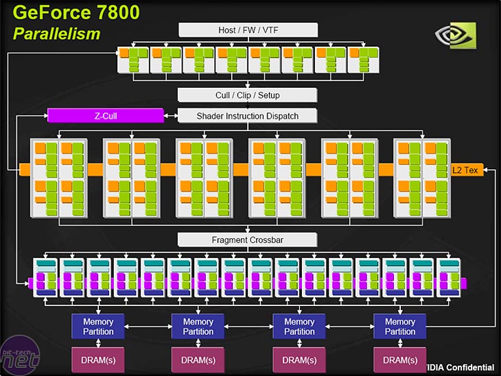 We'll take a look at the individual portions of G70 in a moment, but the basic layout of the graphics-processing unit is as follows:
NV43 was a very shrewd design in that respect, because it allowed NVIDIA to save some die space, and thus cost on a mid-range GPU. G70 follows in its footsteps, saving some die space that is not required, thanks to the way that the Fragment Crossbar 'load balances' the flow of pixels and texels to the array of pixel output engines.
We ran some single-texture fill rate tests on both a G70 and an NV45 at the same clock speeds of 400/1100MHz using software vertex shaders in an attempt to remove any effect that the increased vertex shader count might have on matters. When running a single-texture fill rate test, each pipeline is only given a single pixel/texel to work on in each clock cycle, meaning that the maximum theoretical fill rate that both G70 and NV45 can achieve when clocked at 400MHz is around 3200 Million Pixels per second.
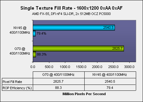 Note: NV45 is the PCI-Express version of NV40, and features the HSI bridge chip on the same packaging as the GPU.
As you can see, the GPU's fill rate does not improve dramatically if you only take the fact that there is a 50% increase in the number of internal 'pixel pipelines'. However, the efficiency of each pixel output engine has gone up by around 9%, meaning that the pixel output engines are doing more work per clock cycle due to the way that the Fragment Crossbar ensures that each pixel output engine is working as much as possible – idle silicon is wasted silicon, right? That is the logic that NVIDIA have taken with GPU design, and we believe that ATI's upcoming R520 will also follow the same logic in that the pixel output engines will be orthogonal in relation to the pixel shader quads.
Where do you spend those extra transistors when you consider that NV40 wasn't exactly a simple graphics-processing unit?
Well, NVIDIA have spent their time improving the efficiency of NV40, and in essence, G70 is from the same parent family as the original NV40, much like the GPU for the upcoming Sony Playstation 3 – they're all based on the same architecture, but NV40 was designed with expansion and efficiency in mind. If you remember back to April last year, the diagram below will ring a bell or two – the flow diagram follows the same basic design principles as NV40, just with more packed in to it.
- 8x Vertex Shaders
- 6x quads of Pixel Shaders – totalling to 24 'pipelines'
- 16x Pixel Output Engines (ROPs)
- 4x 64-bit memory crossbars, adding up to a 256-bit memory interface.
Pixel Output Engine (ROP)
The design has been built around the fundamentals of NV40, but also taking a leaf out of NV43's (GeForce 6600 series') book. You will also notice that there is no increase in the number of pixel output engines - a leaf out of the NV43's book, which had eight internal 'pipelines' and only four pixel output engines. The design worked incredibly well, because of the way that the pixel output engines could write pixels from any of the internal pipelines, meaning that the pixel output engines were able to get closer to their maximum theoretical pixel and texture fill rates.NV43 was a very shrewd design in that respect, because it allowed NVIDIA to save some die space, and thus cost on a mid-range GPU. G70 follows in its footsteps, saving some die space that is not required, thanks to the way that the Fragment Crossbar 'load balances' the flow of pixels and texels to the array of pixel output engines.
We ran some single-texture fill rate tests on both a G70 and an NV45 at the same clock speeds of 400/1100MHz using software vertex shaders in an attempt to remove any effect that the increased vertex shader count might have on matters. When running a single-texture fill rate test, each pipeline is only given a single pixel/texel to work on in each clock cycle, meaning that the maximum theoretical fill rate that both G70 and NV45 can achieve when clocked at 400MHz is around 3200 Million Pixels per second.
As you can see, the GPU's fill rate does not improve dramatically if you only take the fact that there is a 50% increase in the number of internal 'pixel pipelines'. However, the efficiency of each pixel output engine has gone up by around 9%, meaning that the pixel output engines are doing more work per clock cycle due to the way that the Fragment Crossbar ensures that each pixel output engine is working as much as possible – idle silicon is wasted silicon, right? That is the logic that NVIDIA have taken with GPU design, and we believe that ATI's upcoming R520 will also follow the same logic in that the pixel output engines will be orthogonal in relation to the pixel shader quads.


MSI MPG Velox 100R Chassis Review
October 14 2021 | 15:04

Want to comment? Please log in.