The GP104 GPU: Maxwell Architecture, Pascal Refinements
So, how exactly are those 7.2 billion transistors arranged now that we've moved from Maxwell to Pascal? The answer is largely the same. As before, there are groups of Streaming Multiprocessors (SMs) arranged into Graphics Processing Clusters (GPCs). As you can see in the block diagram, Nvidia is also using the term TPC (Texture Processing Cluster) to represent the grouping of a PolyMorph Engine with its SM, but we can ignore this – the pipeline and the various elements that make it up are effectively the same at a high level.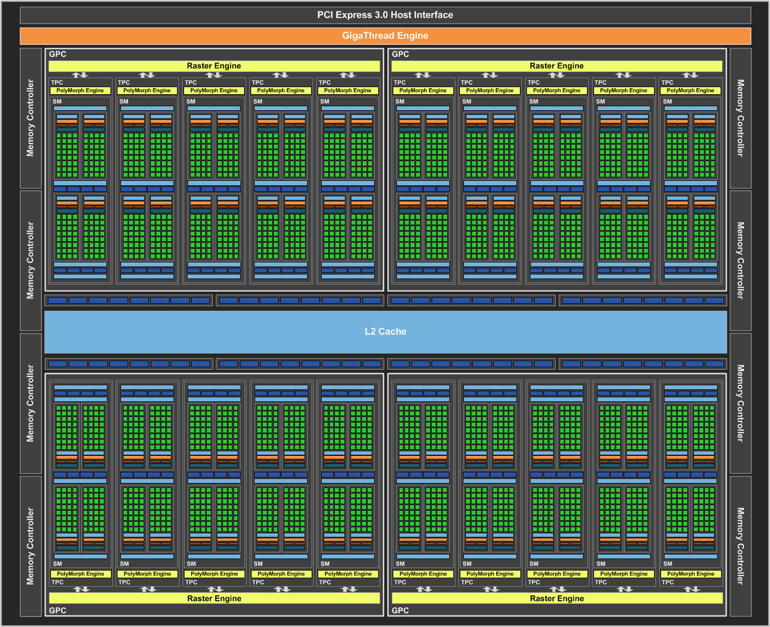
Click to enlarge - The GP104 block diagram
For GP104, which is fully enabled in the GTX 1080, Nvidia uses five SMs per GPC, and there are four GPCs. The highly parallel, power-of-two SM structure remains unchanged and it functions the same, scheduling warps (groups of 32 threads) to the cores, which are arranged in four blocks of 32, each with its own 64KB register file. Each SM also has eight texture units, 48KB of total L1 cache and a 96KB shared memory unit.
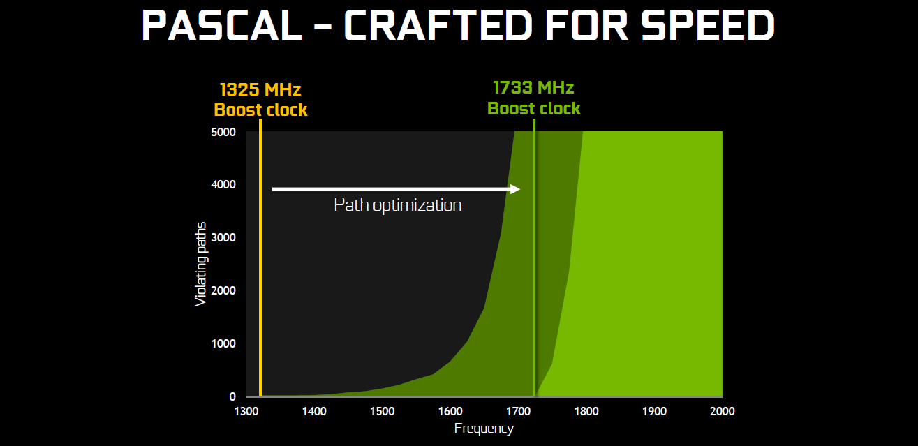
The key thing to note here is that with 20 SMs, the GTX 1080 has 2,560 single-precision CUDA cores at its disposal and 160 texture units. This is already a 25 percent uplift on the GTX 980, all things being equal. Except, all things are not equal, as Nvidia has made improvements elsewhere too. The new process has given Nvidia the headroom to turn up the clock speeds as well, but the firm has also done some critical path analysis on its GPU to really eke the most out of it. You can only increase the clock speed of a chip until the weakest link inside it fails, and there are millions of paths in modern GPUs. By analysing and optimising the critical paths of Pascal, Nvidia has been able to achieve some impressive numbers: the GTX 1080 ships with a base clock of 1,607MHz (1,733MHz boost), which is a new record, and 2GHz and above is supposedly possible with overclocking.
Click to enlarge
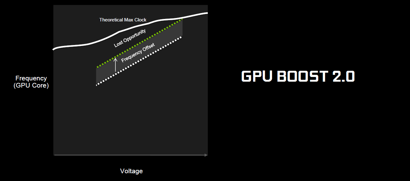
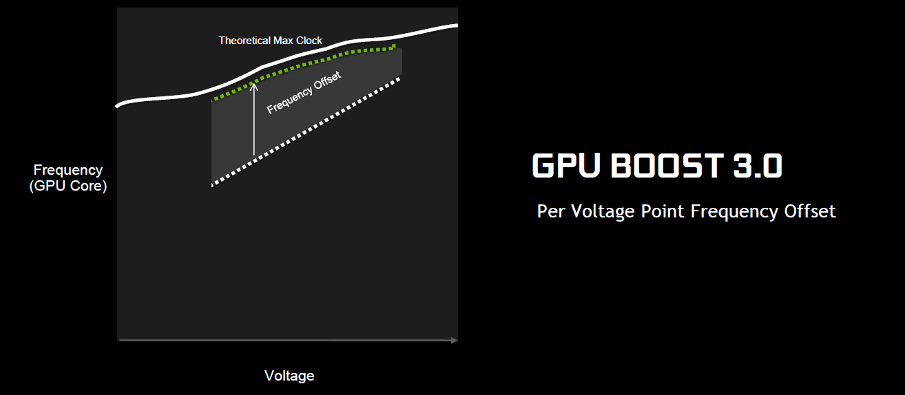
On the topic of clock speed, Nvidia is introducing GPU Boost 3.0 with the GTX 1080. With GPU Boost 2.0, the voltage/frequency curve was offset by a fixed amount, so at any given voltage point the card could only boost up to the set value. However, the voltage/frequency curve varies for each individual GPU and is not linear, so this method involved a certain degree of lost opportunity. Nvidia is looking to combat that now with the introduction of per voltage point frequency offseting. The process can be automated by overclocking utilities, which can examine each point and create a curve specific to your GPU.
Click to enlarge
Click to enlarge
Moving to the back-end, things are largely the same again. There are eight 32-bit memory controllers instead of four 64-bit ones, but this still equates to a 256-bit interface. As usual, each controller is tied to a group of ROPs, eight in this case, and a chunk of L2 cache (256KB), giving us the same totals of 64 ROPs and 2MB L2.
The TDP of the GTX 1080 is 180W, which is actually 15W more than the GTX 980. However, when you consider that it has 25 percent more cores and a 43 percent increase in base clock speed, the efficiency gains of the new process and Nvidia's optimisations are clear, even on paper.


MSI MPG Velox 100R Chassis Review
October 14 2021 | 15:04


Want to comment? Please log in.