
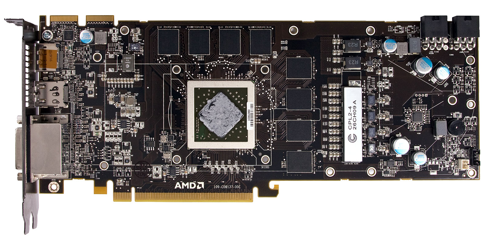
Radeon HD 5870 Power Circuit
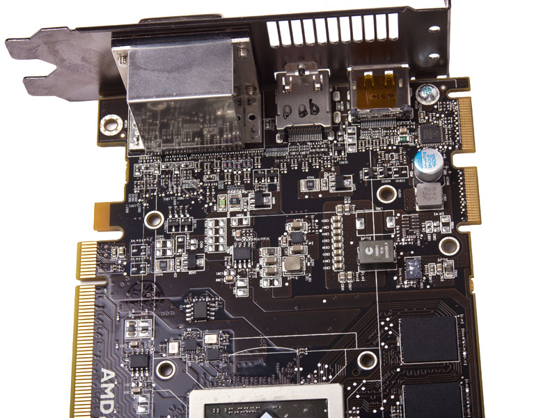
Under the heatsink, there are eight Samsung K4G10325FE-HC04 1Gbit GDDR5 memory chips arranged in an L-shape around the Cypress GPU, making a total of 1GB of memory on the board. These chips are rated to 1,250MHz (5,000MHz effective frequency), which is 50MHz below the speed at which they're set to on the Radeon HD 5870. This means that a standard Radeon HD 5870 card has 1GB of GDDR5 memory running at 1.2GHz (4.8GHz effective).One of the most impressive parts of the card is its power circuitry, which is entirely digital and spread across the PCB. The GPU is powered by four Volterra VT1157SF digital PWMs controlled by a Volterra VT1165MF voltage regulator. As if that's not enough, there are provisions for a fifth phase, should AMD release a faster version of the 5870 later down the line.
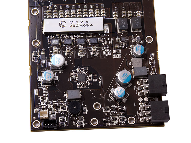
Next to that, there are two tiny Volterra VT242WF PWMs, which supply power to the GDDR5 memory (probably for vDD and vDDQ). Moving around the card, there's a second Volterra VT1165MF voltage regulator paired with another Volterra VT1157SF PWM up next to the CrossFire connectors, which we believe delivers additional power for the memory controller. There's also the provision for a second PWM, should AMD wish to bolster the card's power delivery on a faster card.
Click to enlarge
The two 6-pin PCI Express power connectors supply an additional 150W of power (75W each) in addition to the 75W supplied through the PCI Express slot. AMD says that the Radeon HD 5870's maximum board power is 188W, which is some way below the 225W maximum available power.
Click to enlarge
This gives significant headroom for overclocking and, what's more, there are another two contact points to switch one of the 6-pin connectors for a 150W 8-pin connector. This is further evidence that AMD might release a faster Cypress-based card using the same PCB, but whether AMD chooses to do that will depend on how fast Nvidia's competing GT300-based card ends up being.
Click to enlarge
The Volterra VT1165MF controllers are particularly noteworthy, as they're software controllable. During our conversations with AMD we discovered that these are being used to monitor voltage regulator temperatures, and can reduce the supply voltage or current to prevent overheating. It's fair to say that, with this level of power delivery, the GPU is a bit of a monster.
RELATED ARTICLES


MSI MPG Velox 100R Chassis Review
October 14 2021 | 15:04

Want to comment? Please log in.